Optical cover plate with improved solder mask dam on galss for image sensor package and fabrication method thereof

a technology of image sensor and galss, which is applied in the direction of transportation and packaging, instruments, other domestic objects, etc., can solve the problems of peeling of the prior art package structure, affecting the reliability of component packaging, and high tensile stress of the component packaging, so as to improve the quality of image signal conversion and high reliability. , the effect of high reliability

Active Publication Date: 2011-09-22
XINTEC INC
View PDF15 Cites 6 Cited by
  • Summary
  • Abstract
  • Description
  • Claims
  • Application Information

AI Technical Summary

Benefits of technology

It is another objective of the invention to provide an improved optical cover plate and image sensor package using the same with high reliability and improved quality of image signal conversion.
It is still another objective of the invention to provide a method for fabricating an improved optical cover plate and image sensor package using the same in order to provide high reliability and improved quality of image signal conversion.
According to one embodiment, the annular dam structure is composed of epoxy resins, polyimide, photoresist or silicon-based materials. The transparent substrate comprises glass or quartz. The barrier layer may be a metal layer such as aluminum, aluminum nitride, titanium, titanium nitride, tantalum, tantalum nitride, tungsten, titanium tungsten alloys, silver, gold, or any combination thereof. The barrier layer may be a non-metal layer such as silicon oxide, silicon nitride, silicon oxynitride, silicon carbide, or any combination thereof. The barrier layer prevents moisture from entering the light-receiving region and removes color cast that stems from green color of the annular dam structure.
To sum up, the invention image sensor package and the inventive optical cover plate incorporate a barrier layer on the dam structure, which is capable of resolving color cast problem that stems from the nature and color of the dam structure itself. More importantly, the barrier layer also covers the perimeter of the light-receiving region. By providing such configuration, moisture can be prevented form entering the light-receiving region by way of the annular dam structure. The barrier layer also improves the bonding interface between the annular dam structure and the transparent substrate, the bond pad or the semiconductor substrate. The invention also resolves the peeling problem due to temperature or thermal stress. The invention also provides a method for fabricating the image sensor package and the inventive optical cover plate.

Problems solved by technology

However, the aforementioned prior art package structure, when used in different circumstances, is subject to peeling.
The peeling typically occurs at the interface between the dam structure and the image sensor die and / or the interface between the dam structure and the transparent body because of humidity, stress even the effects of temperature, thereby affecting the reliability of component packaging.
In addition, during the back-end stress test such as high accelerated stress test (HAST), temperature-humidity storage test (THS) or other reliability tests, it has been found that the dam structure itself may absorb moisture, resulting in high tensile stressed component packaging, which reduce production yields.
Further, the color of the dam structure is usually green, there would be image color cast (slightly greenish) issue, which reduces the image quality.
From this, the prior art still has technical issues which need further improvement.

Method used


Image

  • Optical cover plate with improved solder mask dam on galss for image sensor package and fabrication method thereof
  • Optical cover plate with improved solder mask dam on galss for image sensor package and fabrication method thereof
  • Optical cover plate with improved solder mask dam on galss for image sensor package and fabrication method thereof

Examples


Embodiment Construction

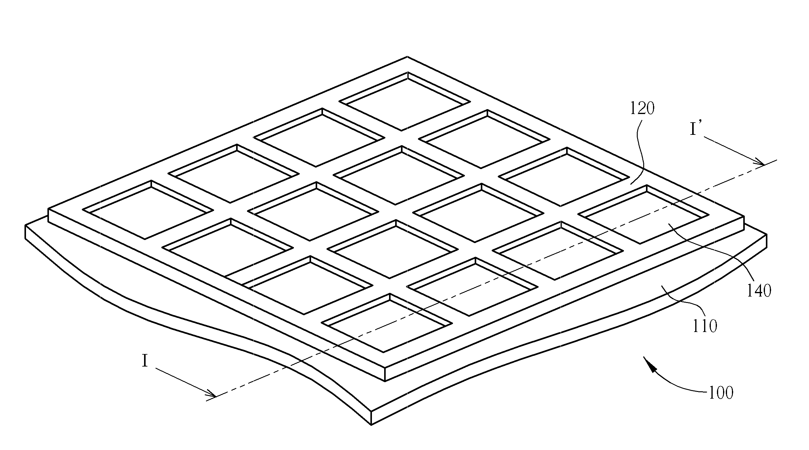
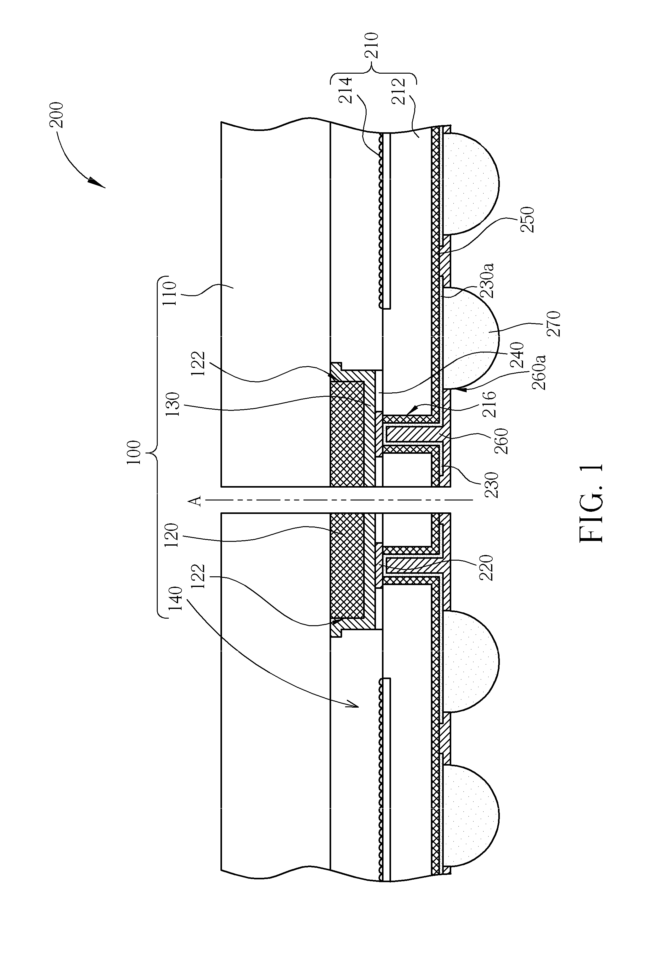
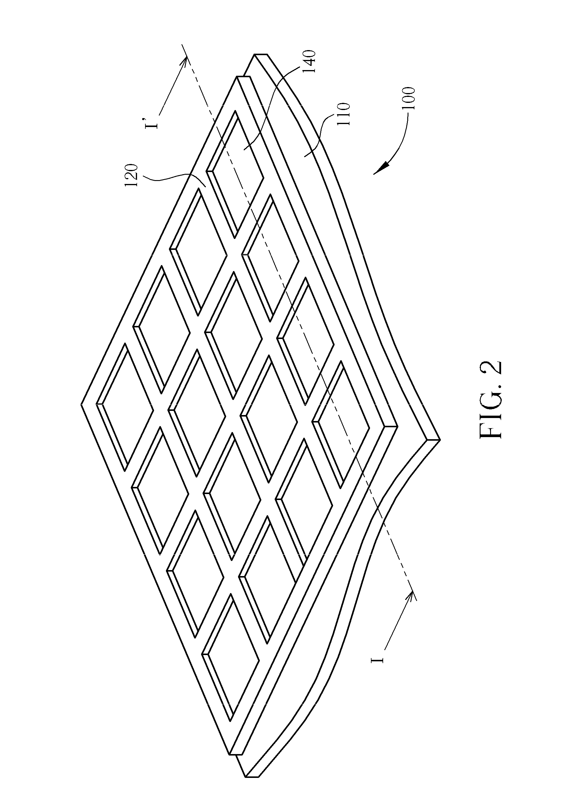
FIG. 1 is a schematic, cross-sectional diagram showing an image sensor package in accordance with one preferred embodiment of this invention. As shown in FIG. 1, generally, the image sensor package 200 is comprised of an optical cover plate 100 and an image sensor die 210. The image sensor die 210 comprises a semiconductor substrate 212, an image sensor device 214 on the active side of the semiconductor substrate 212, a bond pad 220 on the active side of the semiconductor substrate 212, a through-silicon via (TSV) structure 216 penetrating through of the semiconductor substrate 212, an insulating layer 250 on the backside of the semiconductor substrate 212, and a metal layer 230 on the insulating layer 250 for electrically connecting the bond pad 220. The metal layer 230 is conformally deposited in the TSV structure 216 and forms a re-distribution layer (RDL) including a solder pad pattern 230a on the backside of the semiconductor substrate 212. A solder mask 260 is formed on the me...


PUM

PropertyMeasurementUnit
transparentaaaaaaaaaa
green coloraaaaaaaaaa
sizeaaaaaaaaaa

Abstract

An optical cover plate for image sensor package includes a transparent substrate, at least an annular dam structure, and a barrier layer. The annular dam structure is disposed on the transparent substrate and encompasses a light-receiving area. The barrier layer conformally covers at least a sidewall of the annular dam structure. A method of manufacturing the optical cover plate, an image sensor package and fabrication method thereof are also disclosed.

Description

BACKGROUND OF THE INVENTION1. Field of the InventionThe present invention relates generally to image sensor packaging. More particularly, the present invention relates to an optical cover plate for image sensor wafer level package and fabrication method thereof. The invention optical cover plate includes an improved dam structure. Further, the invention provides an image sensor package using the same and fabrication method thereof.2. Description of the Prior ArtWith the development and popularity of electronic products such as digital cameras, mobile phones, personal computers and scanners, the image sensor devices have been widely used in various fields. The commonly used solid-state image sensor devices can be generally categorized into two types: charge-coupled device (CCD) and CMOS image sensor. As known in the art, the CMOS image sensors are compatible with semiconductor manufacturing process to achieve low-cost manufacturing. The CMOS image sensors also provide advantages such...

Claims


Application Information

Patent Timeline
Patent Type & Authority Applications(United States)
IPC IPC(8): G02B27/00C23F1/00
CPCH01L27/14618H01L2924/0002H01L23/481H01L24/05H01L24/13H01L2224/02372H01L2224/05548H01L2224/05567H01L2224/13022H01L2224/13024H01L2224/131H01L2224/94H01L27/14687H01L2224/0401H01L2224/11H01L2224/03H01L2924/014H01L2224/05552
Inventor LIN, CHIA-SHENG
Owner XINTEC INC
Why Eureka
Try Eureka