Hybrid combination of substrate and carrier mounted light emitting devices

a light-emitting device and carrier-mounted technology, which is applied in the direction of semiconductor/solid-state device manufacturing, semiconductor devices, electrical equipment, etc., can solve the problems of increasing the manufacturing cost of led elements, manufacturing limitations and quality control limitations that do not allow tile use, etc., to achieve lower cost multi-chip, improve reliability and/or operational life, and improve the effect of effective yield

Active Publication Date: 2011-09-29
LUMILEDS
View PDF20 Cites 12 Cited by
  • Summary
  • Abstract
  • Description
  • Claims
  • Application Information

AI Technical Summary

Benefits of technology

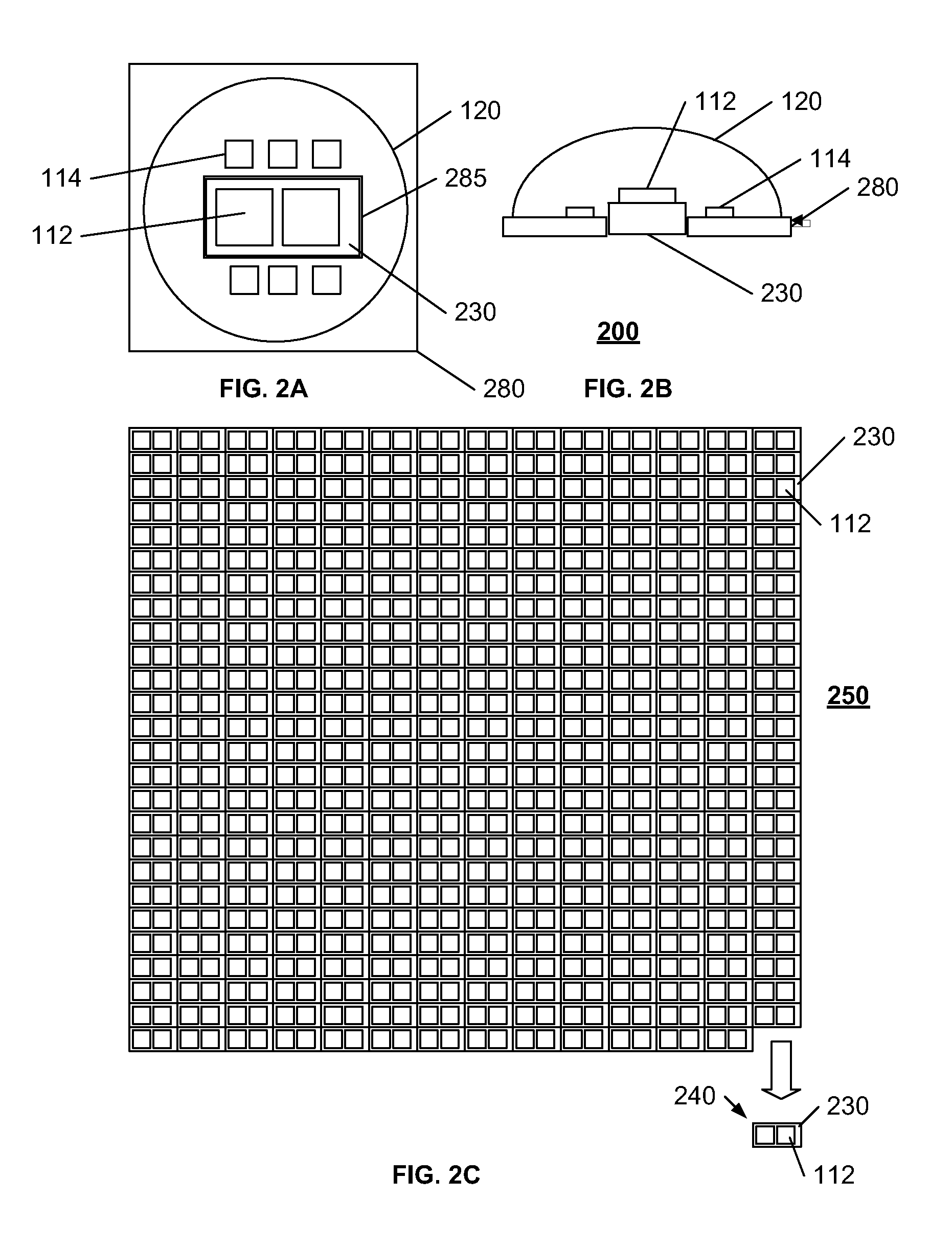
[0012]It would be advantageous to provide a lower cost multi-chip encapsulation product. It would also be advantageous to allow for interconnected elements on the undiced substrate tile while avoiding the additional application of a protective layer after the substrate is diced. It would also be advantageous to provide a multi-chip encapsulation product with higher reliability and / or longer operational life. It would also be advantageous to provide a multi-chip encapsulation product with a higher effective yield. It would also be advantageous to allow for the concurrent production of more devices per processing stage.
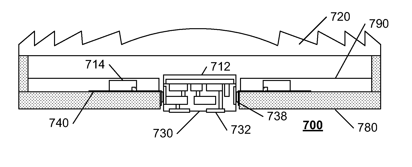
[0013]These advantages, and others, may be realized by a low-cost carrier structure that facilitates the encapsulation process while accommodating substrates that are optimized to support the devices that require a substrate. Depending upon the type of LED elements used, some of the LED elements may be mounted on the carrier structure, rather than on the more expensive ceramic substrate. In like manner, other devices, such as sensors and control elements, may be mounted on the carrier structure as well. Advantageously, the devices that are mounted on the carrier structure may be thermally separated from the substrate. Because the carrier and substrate structures are formed independent of the encapsulation and other after-formation processes, these structures can be tested prior to encapsulation, thereby avoiding the cost of these processes being applied to inoperative structures.

Problems solved by technology

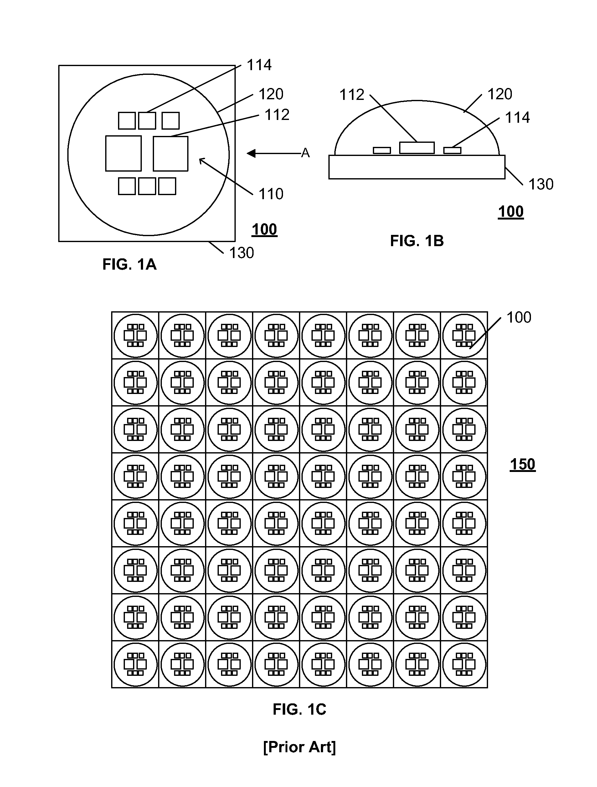
However, manufacturing limitations and quality control limitations do not currently allow for the use of tiles much larger than 100 mm×100 mm.
Because of this requirement, an additional protective layer may be applied to or over each LED element 100 after it is diced from the tile 150, to insulate any exposed connections, thereby increasing the manufacturing costs for such LED elements 100.

Method used


Image

  • Hybrid combination of substrate and carrier mounted light emitting devices
  • Hybrid combination of substrate and carrier mounted light emitting devices
  • Hybrid combination of substrate and carrier mounted light emitting devices

Examples


Embodiment Construction

[0023]In the following description, for purposes of explanation rather than limitation, specific details are set forth such as the particular architecture, interfaces, techniques, etc., in order to provide a thorough understanding of the concepts of the invention. However, it will be apparent to those skilled in the art that the present invention may be practiced in other embodiments, which depart from these specific details. In like manner, the text of this description is directed to the example embodiments as illustrated in the Figures, and is not intended to limit the claimed invention beyond the limits expressly included in the claims. For purposes of simplicity and clarity, detailed descriptions of well-known devices, circuits, and methods are omitted so as not to obscure the description of the present invention with unnecessary detail.

[0024]Also in the following description, commonly used materials and processes are referenced to facilitate better and / or easier understanding o...


PUM

PropertyMeasurementUnit
wavelengthaaaaaaaaaa
surface areaaaaaaaaaaa
thermal propagation characteristicsaaaaaaaaaa

Abstract

A multi-chip light emitting device (LED) uses a low-cost carrier structure that facilitates the use of substrates that are optimized to support the devices that require a substrate. Depending upon the type of LED elements used, some of the LED elements may be mounted on the carrier structure, rather than on the more expensive ceramic substrate. In like manner, other devices, such as sensors and control elements, may be mounted on the carrier structure as well. Because the carrier and substrate structures are formed independent of the encapsulation and other after-formation processes, these structures can be tested prior to encapsulation, thereby avoiding the cost of these processes being applied to inoperative structures.

Description

[0001]This application is a continuation-in-part of U.S. patent application Ser. No. 12 / 731,501, filed 25 Mar. 2010, the contents of which is incorporated by reference herein.BACKGROUND[0002]This invention relates to the field of Integrated Circuit (IC) fabrication and assembly, and in particular to the fabrication of an encapsulated multi-chip device, such as a multi-die LED with an integral encapsulation lens.[0003]As the light emitting capabilities of solid state light emitting devices1 (LEDs) continues to improve, their use in conventional lighting applications continues to increase, as does the competitive pressures to provide reliable, long-lasting products in a cost-effective manner. Even though the cost of LED products is relatively low, the savings of even a few cents per device can have a significant impact on profit margin, due to the increasingly growing market for these devices. 1 For the purposes of this disclosure, the acronym ‘LED’ refers to a light emitting device; ...

Claims


Application Information

Patent Timeline
Patent Type & Authority Applications(United States)
IPC IPC(8): H01L33/08H01L21/78
CPCH01L2224/48091H01L33/54H01L25/0753H01L2924/09701H01L31/12H01L33/58H01L33/52H01L2924/00014
Inventor BIERHUIZEN, SERGE J.
Owner LUMILEDS
Why Eureka
Try Eureka