Solid-state image pickup element and image pickup apparatus

a pickup element and solid-state technology, applied in the direction of television system scanning details, radioation control devices, television systems, etc., can solve problems such as deteriorating image quality, and achieve the effect of satisfying image quality, and suppressing or preventing the generation of dark currents

Active Publication Date: 2011-09-29
SONY CORP
View PDF3 Cites 15 Cited by
  • Summary
  • Abstract
  • Description
  • Claims
  • Application Information

AI Technical Summary

Benefits of technology

[0042]As a result, the impurity region of the first conductivity type acts as a potential barrier against a minority carrier (electron or hole) injected from the contact portion. Thus, it is possible to suppress or prevent the flowing of the minority carrier into the photoelectric conversion region.
[0043]Therefore, it is possible to suppress or prevent the generation of the dark current due to the flowing of the minority carrier into the photoelectric conversion region.
[0052]The provision of the barrier makes it possible to suppress or prevent the flowing of the minority carrier into the photoelectric conversion region.
[0053]Therefore, it is possible to suppress or prevent the generation of the dark current due to the flowing of the minority carrier into the photoelectric conversion region.
[0062]According to the image pickup apparatus of still another embodiment or yet another embodiment of the present invention, the image pickup apparatus includes the solid-state image pickup element of the embodiment or the solid-state image pickup element of another embodiment. Therefore, it is possible to suppress or prevent the generation of the dark current due to the flowing of the minority carrier into the photoelectric conversion region.
[0063]As set forth hereinabove, according to the present invention, since it is possible to suppress or prevent the generation of the dark current due to the flowing of the minority carrier into the photoelectric conversion region, it is possible to realize a solid-state image pickup element for obtaining satisfactory image quality, and a high definition image pickup apparatus including the same.

Problems solved by technology

In this structure, however, there is known a problem that electrons e− as minority carriers are injected from the well contact 68 to the p-type region 77.
That is to say, this problem is such that as indicated by arrows in FIGS. 23 and 24, respectively, the injected electrons e− are diffused within the p-type region 77 to flow into the n-type region 73 in which the electrons generated in the photodiode by the photoelectric conversion are accumulated, and turn into a dark current, thereby deteriorating the image quality.

Method used


Image

  • Solid-state image pickup element and image pickup apparatus
  • Solid-state image pickup element and image pickup apparatus
  • Solid-state image pickup element and image pickup apparatus

Examples


first embodiment

2. First Embodiment

[0134]Subsequently, concrete embodiments of the present invention will be described below.

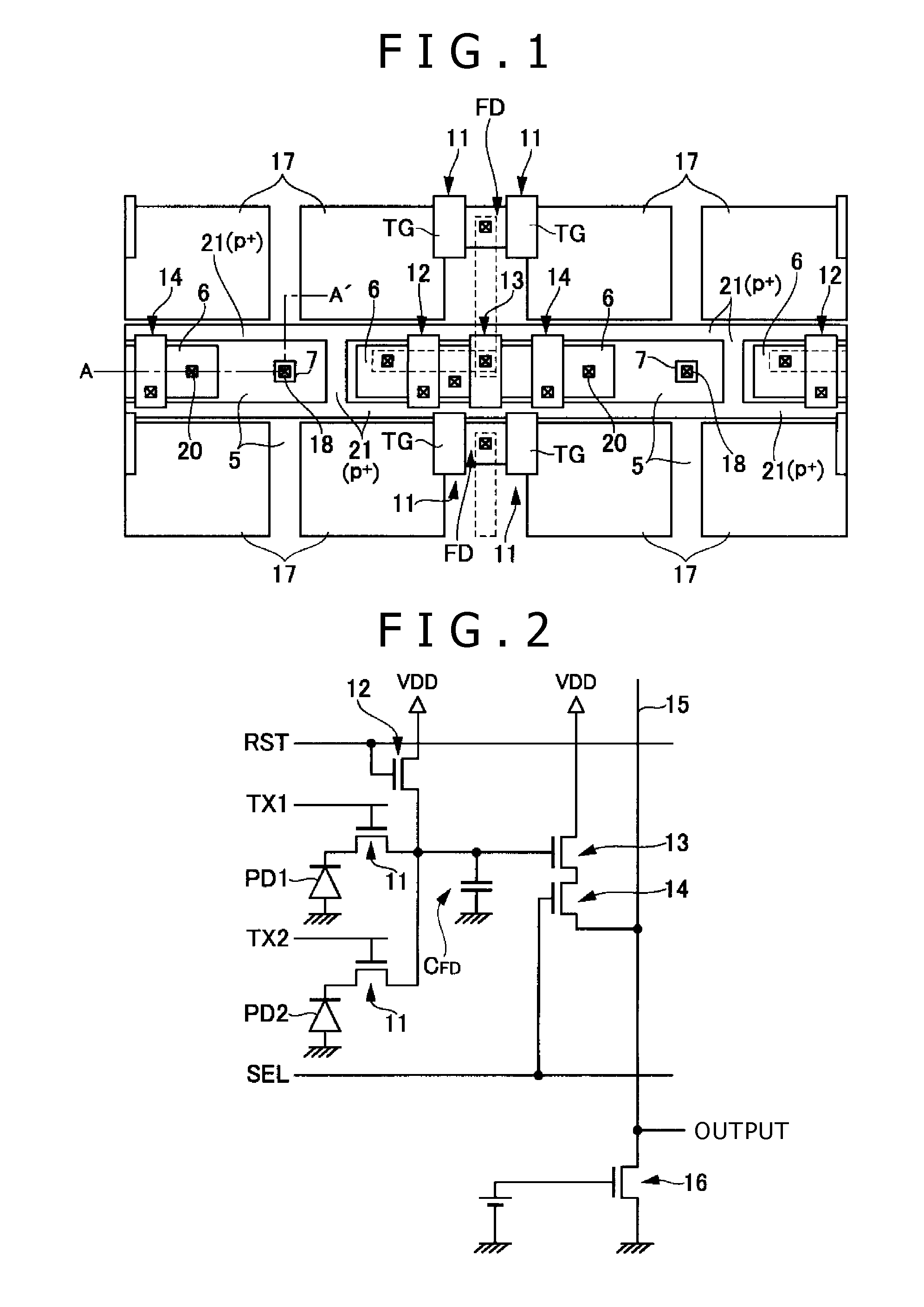
[0135]FIG. 1 is a top plan view showing a schematic structure of a main portion of a solid-state image pickup element according to a first embodiment of the present invention. Also, FIG. 1 shows a top plan view of a part (two pixel length×four pixels width) of an image pickup area of the solid-state image pickup element.

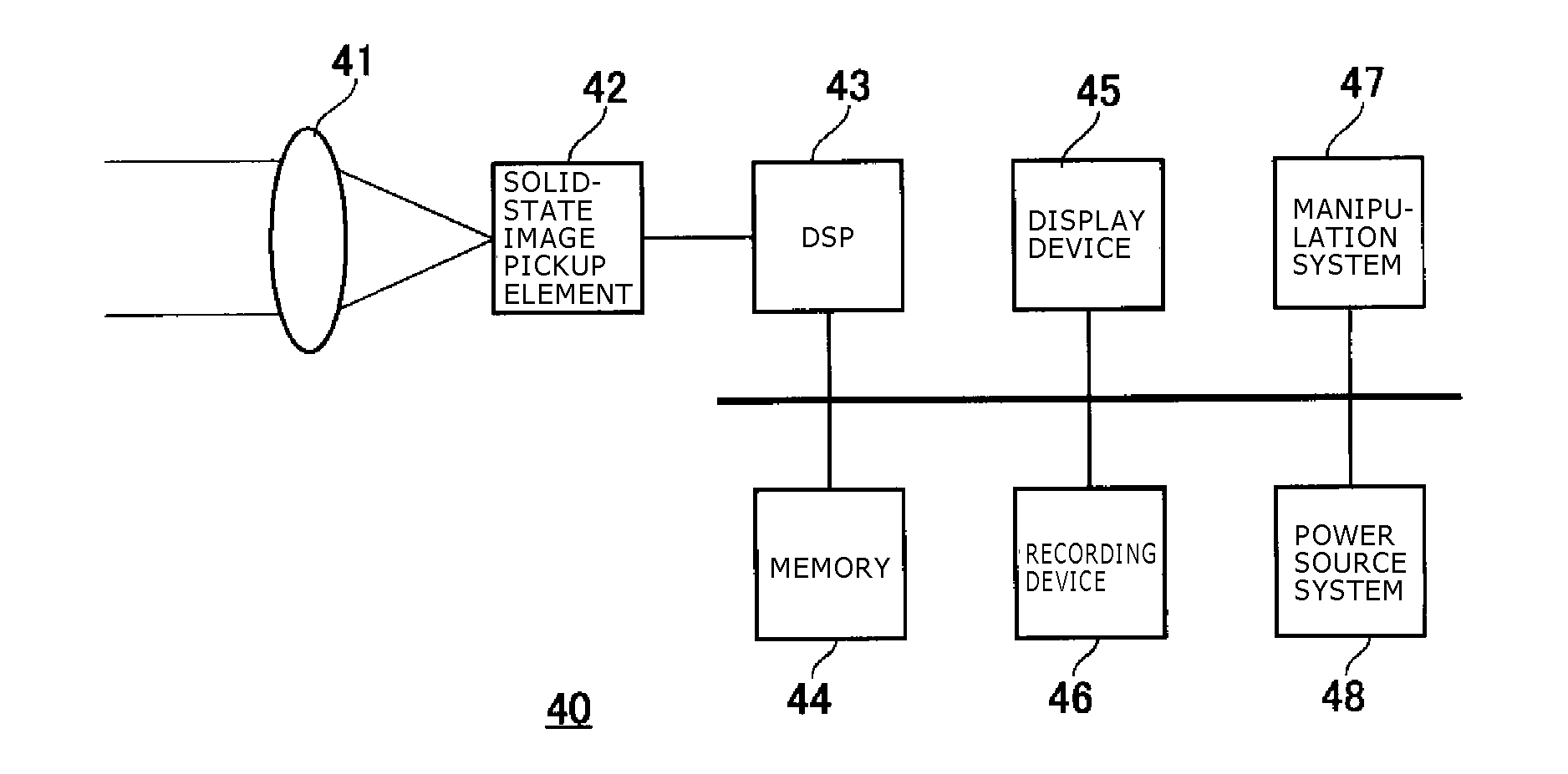
[0136]It is noted that the entire configuration of the solid-state image pickup element can be made identical to that shown in FIG. 20.

[0137]As shown in FIG. 1, a photoelectric conversion region 17 including a photodiode is formed in each of pixels. Three transistors of a reset transistor 12, an amplification transistor 13, and a selection transistor 14 are formed continuously as a set between the photoelectric conversion regions 17 of the pixels in an upper row, and the photoelectric conversion regions 17 of the pixels in a lower row.

[0138]A well contact 18 i...

second embodiment

3. Second Embodiment

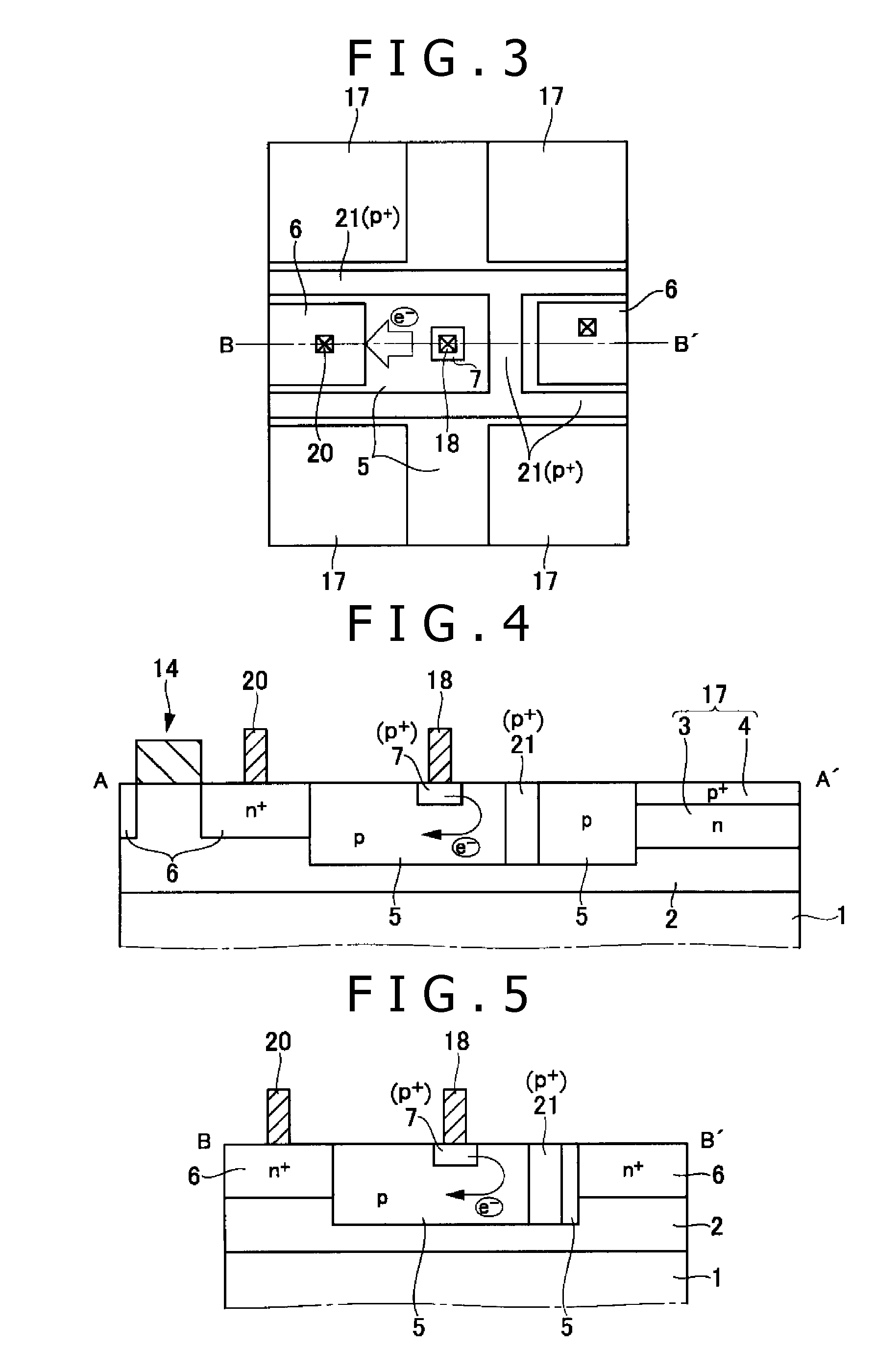
[0180]FIG. 7 is a top plan view showing a schematic structure of a main portion of a solid-state image pickup element according to a second embodiment of the present invention. Also, FIG. 8 is an enlarged top plan view showing a structure of a portion in the vicinity of a well contact shown in FIG. 7.

[0181]In the second embodiment, the p+-type region 21 serving as the barrier is formed between the well contact 18 and the photoelectric conversion region 17.

[0182]That is to say, the p+-type region 21 is not formed between the n+-type region 6 of the reset transistor 12, and the well contact 18, although the p+-type region 21 is formed there in the first embodiment.

[0183]As a result, as indicated by arrows of FIG. 8, the electrons e− generated from the well contact 18 flow into the n+-type regions 6 at the both right and left sides of the well contact 18.

[0184]Since other structures in the second embodiment are the same as those in the first embodiment shown in FIGS...

third embodiment

4. Third Embodiment

[0189]FIG. 9 is a top plan view showing a schematic structure of a main portion of a solid-state image pickup element according to a third embodiment of the present invention. Also, FIG. 10 is a cross sectional view taken on line C-C′ of FIG. 9.

[0190]In the third embodiment, the disposition of the transistors within the pixel area is changed, whereby the n+-type regions 6 which are connected to power sources VDD, respectively, are disposed close to the well contact 18 so as to face both sides of the well contact 18, respectively.

[0191]That is to say, in the first embodiment, the three transistors 12, 13 and 14 are disposed as the continuous one set. On the other hand, in the third embodiment, as shown in FIG. 9, the reset transistor 12 is disposed independently of other two transistors, that is, the amplification transistor 13 and the selection transistor 14. In addition, of the two n+-type regions 6 of the reset transistor 12 and the amplification 13, the p+-type...


PUM


Abstract

Disclosed herein is a solid-state image pickup element, including: a photoelectric conversion region; a transistor; an isolation region of a first conductivity type configured to isolate the photoelectric conversion region and the transistor from each other; a well region of the first conductivity type having the photoelectric conversion region, the transistor, and the isolation region of the first conductivity type formed therein; a contact portion configured to supply an electric potential used to fix the well region to a given electric potential; and an impurity region of the first conductivity type formed so as to extend in a depth direction from a surface of the isolation region of the first conductivity type in the isolation region of the first conductivity type between the contact portion and the photoelectric conversion region, and having a sufficiently higher impurity concentration than that of the isolation region of the first conductivity type.

Description

BACKGROUND OF THE INVENTION[0001]1. Field of the Invention[0002]The present invention relates to a solid-state image pickup element and an image pickup apparatus, such as a camera, including the same.[0003]2. Description of the Related Art[0004]A configuration including a photodiode utilizing a pn junction of a semiconductor as a photoelectric conversion element is known for a solid-state image pickup element (image sensor) using a semiconductor.[0005]Such a solid-state image pickup element is mounted to many apparatuses such as a digital camera, a video camera, a monitoring camera, a copying machine, and a facsimile.[0006]Also, a so-called CMOS (complementary metal oxide semiconductor) type solid-state image pickup element which is manufactured in a CMOS process, including a peripheral circuit is used as such a solid-state image pickup element in many cases.[0007]FIG. 20 is a schematic block diagram showing an example of a configuration of a CMOS type solid-state image pickup eleme...

Claims


Application Information

Patent Timeline
Patent Type & Authority Applications(United States)
IPC IPC(8): H04N5/335H01L27/146
CPCH01L27/14603H01L27/1461H01L27/1463H01L31/06H01L27/14689H01L31/02327H01L27/14641H01L27/14612H01L27/14634H01L27/14636H01L27/14643Y02E10/50
Inventor YAMAKAWA, SHINYA
Owner SONY CORP
Why Eureka
Try Eureka