

MEMS device
a technology of a fuse element and a fuse element, which is applied in the direction of semiconductor devices, semiconductor device details, electrical apparatus, etc., can solve the problems of increasing the amount of current necessary for blowing the fuse element, hard for a heat generated by the fuse element, and the characteristics of the fuse element are not stabilized, so as to achieve the effect of stabilizing the characteristics of the fuse elemen
- Summary
- Abstract
- Description
- Claims
- Application Information
AI Technical Summary
Benefits of technology
Problems solved by technology
Method used
Image

Examples
first modified example
[0073](1) First modified example
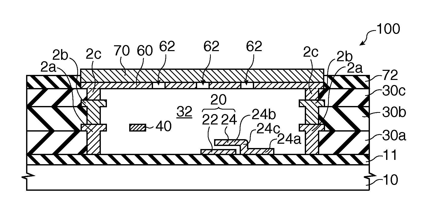
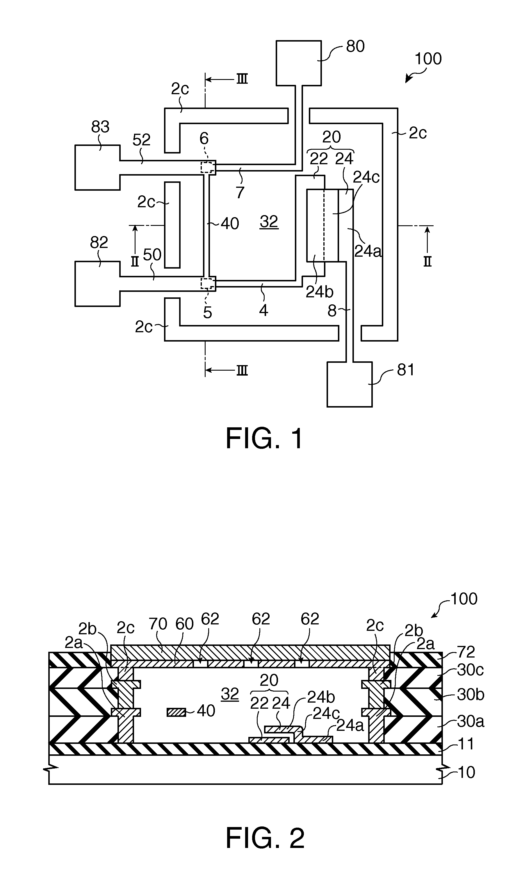
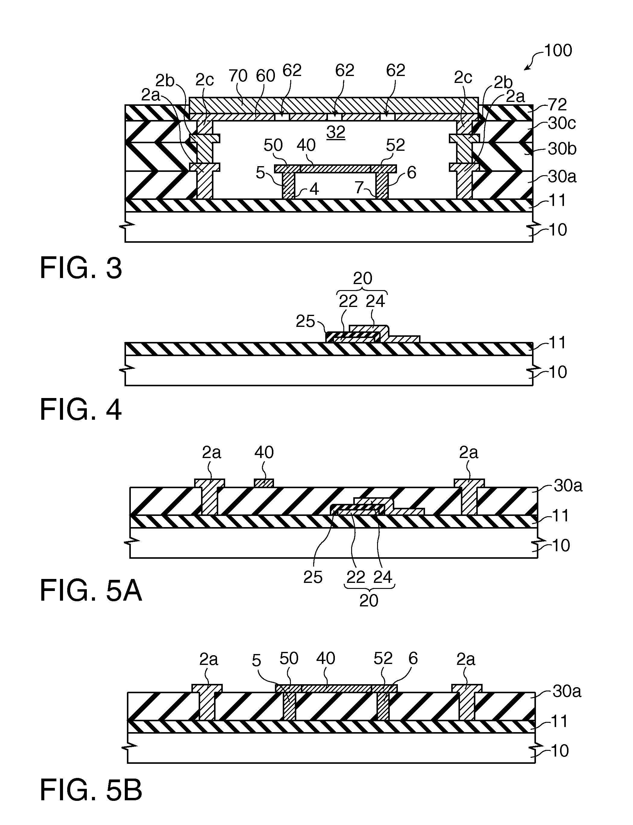
[0074]First, a MEMS device 200 according to a first modified example of the embodiment will be described. FIG. 9 is a plan view schematically showing the MEMS device 200. FIG. 10 is a cross-sectional view schematically showing the MEMS device 200 taken along line X-X of FIG. 9. FIGS. 11 and 12 are plan views schematically showing other examples of the MEMS device 200. In FIGS. 9, 11, and 12, the illustrations of the substrate 10, the insulating layer 11, the inter-layer insulating layers 30a, 30b, and 30c, the first covering layer 60, the second covering layer 70, and the protective film 72 are omitted for convenience.
[0075]As shown in FIGS. 9 and 10, the MEMS device 200 can have a wall section 210 formed between the functional element 20 and the fuse element 40 on the insulating layer 11 of the substrate 10.
[0076]As shown in FIG. 10, the wall section 210 is composed of a first portion 210a formed on the insulating layer 11 and a second portion 210b f...
second modified example
[0079](2) Second modified example
[0080]Next, a MEMS device 300 according to a second modified example of the embodiment will be described. FIG. 13 is a plan view schematically showing the MEMS device 300. In FIG. 13, the illustrations of the substrate 10, the insulating layer 11, the inter-layer insulating layers 30a, 30b, and 30c, the first covering layer 60, the second covering layer 70, and the protective film 72 are omitted for convenience.
[0081]In the example of the MEMS device 100 as shown in FIGS. 1 and 2, the functional element 20 and the fuse element 40 are included. As shown in FIG. 13, on the other hand, the MEMS device 300 can further have, in addition to the functional element 20 and the fuse element 40, another functional element 320 contained in the cavity 32 and another fuse element 340 contained in the cavity 32 and electrically connected with the functional element 320.
[0082]In the illustrated example, the two functional elements 20 and 320 and the two fuse element...
third modified example
[0085](3) Third modified example
[0086]Next, a MEMS device 400 according to a third modified example of the embodiment will be described. FIG. 14 is a plan view schematically showing the MEMS device 400. FIG. 15 is a cross-sectional view schematically showing the MEMS device 400 taken along line XV-XV of FIG. 14. In FIG. 14, the illustrations of the substrate 10, the insulating layer 11, the inter-layer insulating layers 30a, 30b, and 30c, the first covering layer 60, the second covering layer 70, and the protective film 72 are omitted for convenience.
[0087]In the MEMS device 400, the functional element 20 and the fuse element 40 are formed on the insulating layer 11. Thus, without forming the interconnect plugs 5 and 6 (refer to FIGS. 1 and 3), the fuse element 40 can be formed spaced apart from the substrate 10. Therefore, compared to the example of the MEMS device 100, the manufacturing steps can be simplified.
[0088]In the MEMS device 400, similarly to the MEMS device 100, compare...
PUM
 Abstract
Description
Claims
Application Information