

Solid-state imaging device and driving method as well as electronic apparatus
a technology of solid-state imaging and driving method, which is applied in the direction of instruments, television systems, and scanning details of television systems, can solve problems such as bad influence on signal reading, and achieve the effects of reducing noise generation, reducing noise, and high simultaneity in degree of freedom
Active Publication Date: 2011-10-06
SONY SEMICON SOLUTIONS CORP
View PDF11 Cites 18 Cited by
- Summary
- Abstract
- Description
- Claims
- Application Information
AI Technical Summary
Benefits of technology
The patent text describes a problem in the operation of a solid-state imaging device where the simultaneous driving of overflow gates can affect the reading of signals from the pixels. To address this problem, the patent proposes a method for carrying out the simultaneous driving of the overflow gates during a specific period of time, called an "operation timing." By doing this, the negative effects of simultaneous driving can be minimized and the overall image quality can be improved. The patent also discusses a method for allocating the reading and A / D conversion operations to the overall area of a row period, which allows for a longer period of time for the overlap of signals between rows. Overall, the patent provides a solution for improving the performance and quality of solid-state imaging devices.
Problems solved by technology
Method used
View moreImage
Smart ImageViewing Examples

Examples
first embodiment (
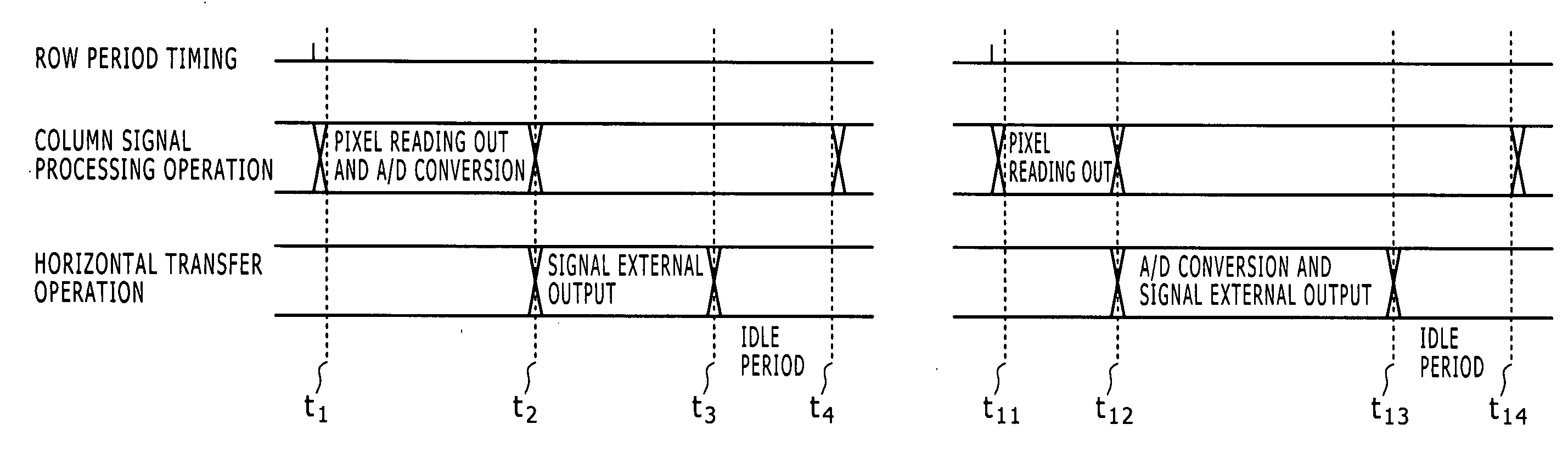
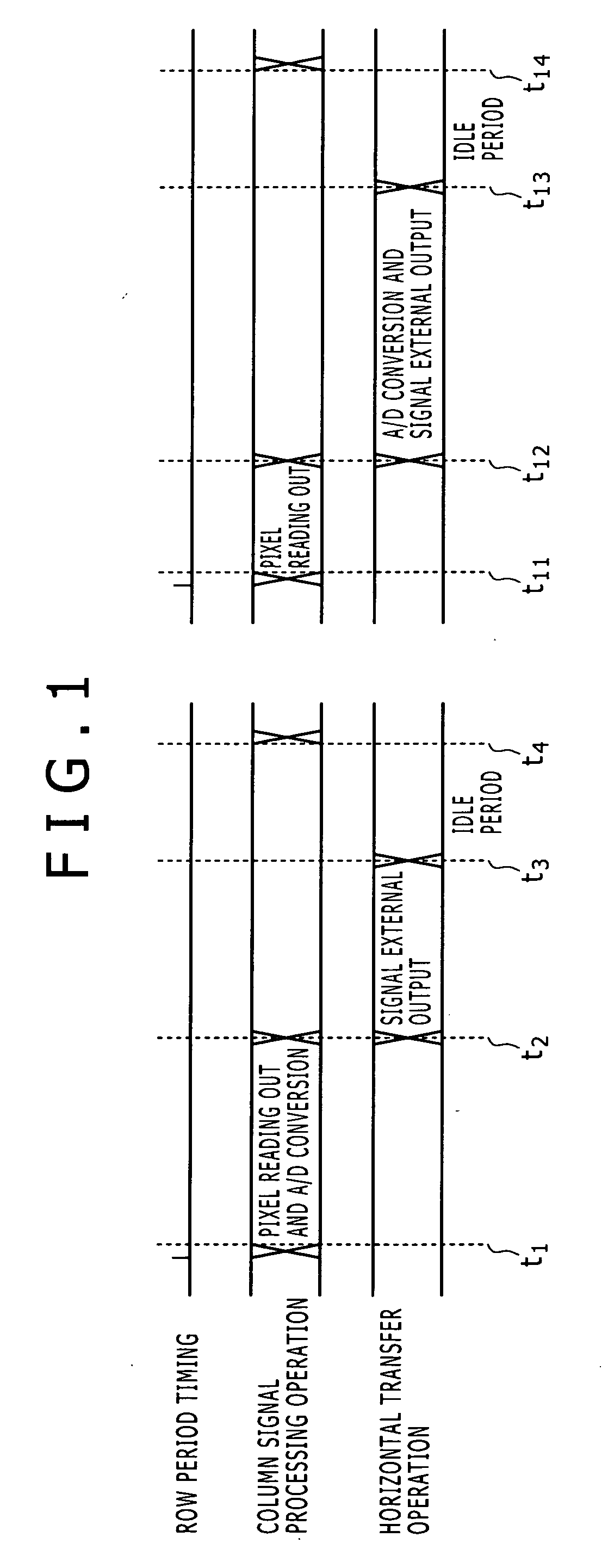
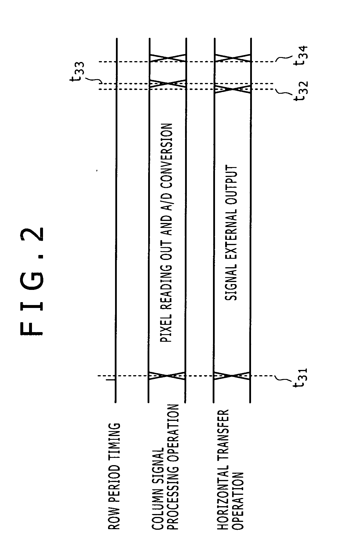
1. First Embodiment (example of a configuration wherein a dummy row is provided)
second embodiment (
2. Second Embodiment (example of a configuration wherein no dummy row is provided)
third embodiment (
3. Third Embodiment (example of a configuration wherein a selector is provided)
Login to View More PUM
| Property | Measurement | Unit |
|---|---|---|
| charge | aaaaa | aaaaa |
| speed | aaaaa | aaaaa |
| area | aaaaa | aaaaa |
Abstract
A solid-state imaging device includes: a CMOS image sensor including a plurality of pixels disposed in an array and each including a light reception element, a discharging unit, a charge accumulation section, a transfer unit, a reset unit, an amplification unit, and a selection unit; and a control unit adapted to generate a selection pulse for rendering the selection unit operative to control operation of the CMOS image sensor.
Description
BACKGROUND OF THE INVENTION[0001]1. Field of the Invention[0002]This invention relates to a solid-state imaging device and a driving method for a solid-state imaging device as well as an electronic apparatus, and more particular to a technique for reducing generation of noise in a solid-state imaging device and a driving method for a solid-state imaging device as well as an electronic apparatus.[0003]2. Description of the Related Art[0004]A popular image sensor of the CMOS (Complementary Metal Oxide Semiconductor) type includes a mechanism for sequentially scanning a pixel array, in which pixels are arrayed two-dimensionally, for each pixel row to carry out reading out. This row-sequential scanning generates a displacement in time among accumulation periods with regard to different pixel rows and gives rise to occurrence of a phenomenon called focal plane distortion that a picked up image upon imaging of a moving imaging object is distorted.[0005]In imaging applications to an imagin...
Claims
Login to View More Application Information
Patent Timeline
 Patent Type & AuthorityApplications(United States)
IPC IPC(8): H04N5/335H04N25/00H04N25/65
CPCH01L27/14609H01L27/14643H01L27/14656H04N5/357H04N5/3592H04N5/361H04N5/3532H04N25/531H04N25/622H04N25/63H04N25/672H04N25/60
InventorKATO, AKIHIKOOIKE, YUSUKE
OwnerSONY SEMICON SOLUTIONS CORP