Filter based on a combined via structure

Active Publication Date: 2011-10-13
NEC CORP
View PDF1 Cites 9 Cited by
  • Summary
  • Abstract
  • Description
  • Claims
  • Application Information

AI Technical Summary

Benefits of technology

[0008]In an aspect of the present invention, such combined via structure is provided by disposing two working parts arranged in vertical direction (perpendicular to multilayer board conductor plane) one after another. The first working part is used for low-loss signal transmission. This working part is formed by signal and ground vias connected to ground plates which are separated by the clearance hole. In this functional part, characteristic impedance control is provided by transverse dimensions of the signal via, the distance between signal via and ground vias, and also by dimensions of the clearance hole. The second working part is applied to obtain short-circuited or open-circuited resonance stub in a multilayer board. This working part is also formed by signal and ground vias connected to ground planes. However, this working part uses specific corrugated plates connected to the signal via and separated by isolating slits from other conductors. These conductive plates give a possibility to control characteristic impedance and propagation constant of the second working part by means of their form and dimensions and achieve required resonant frequencies of the stubs. Besides that, corrugations of the side edges of the plates are used to reduce transverse dimensions of the combined via structures.
[0009]It is another objective of this invention to provide filters, using invented combined via structures in multilayer boards, and, as a result, to reduce whole transverse dimensions of the filters and their hand-pass and band-stop performances such as sharpness.

Problems solved by technology

In this case, parasitic coupling, unwanted radiation and large enough dimensions can be those issues, which can arise at development of distributed-element devices.

Method used


Image

  • Filter based on a combined via structure
  • Filter based on a combined via structure
  • Filter based on a combined via structure

Examples


Embodiment Construction

[0064]Hereinafter, several types of combined via structures and compact filters based on these via structures disposed in multilayer boards according to the present invention will be described in detail with reference to attached drawings. But, it would be well understood that this description should not be viewed as narrowing the appended claims.

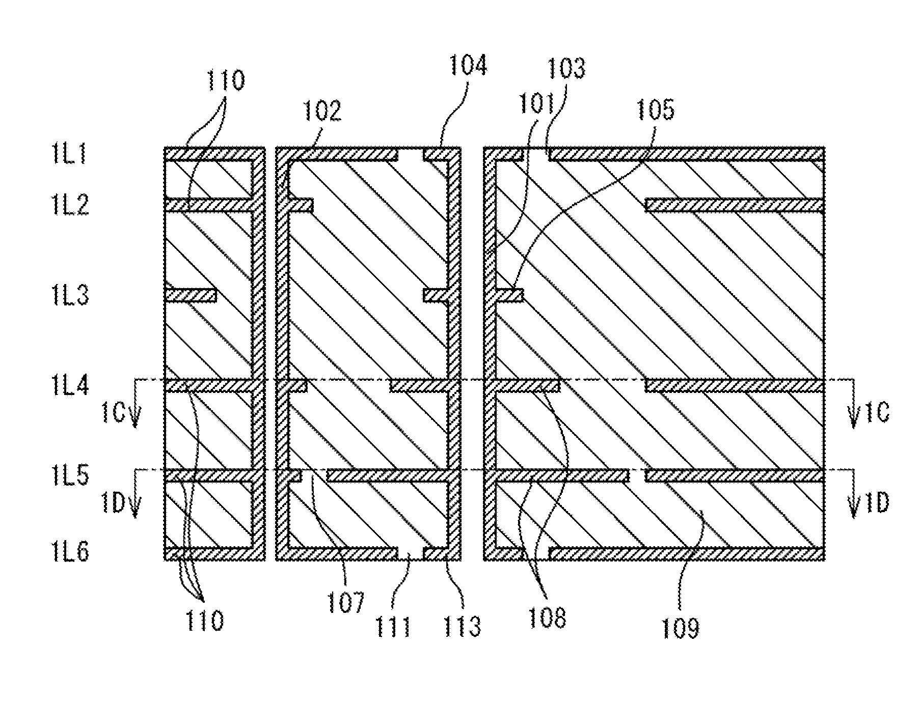
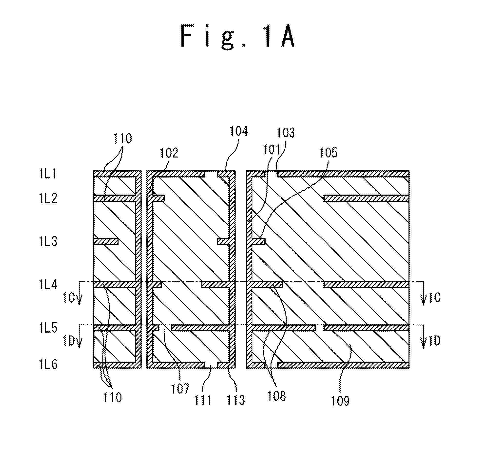
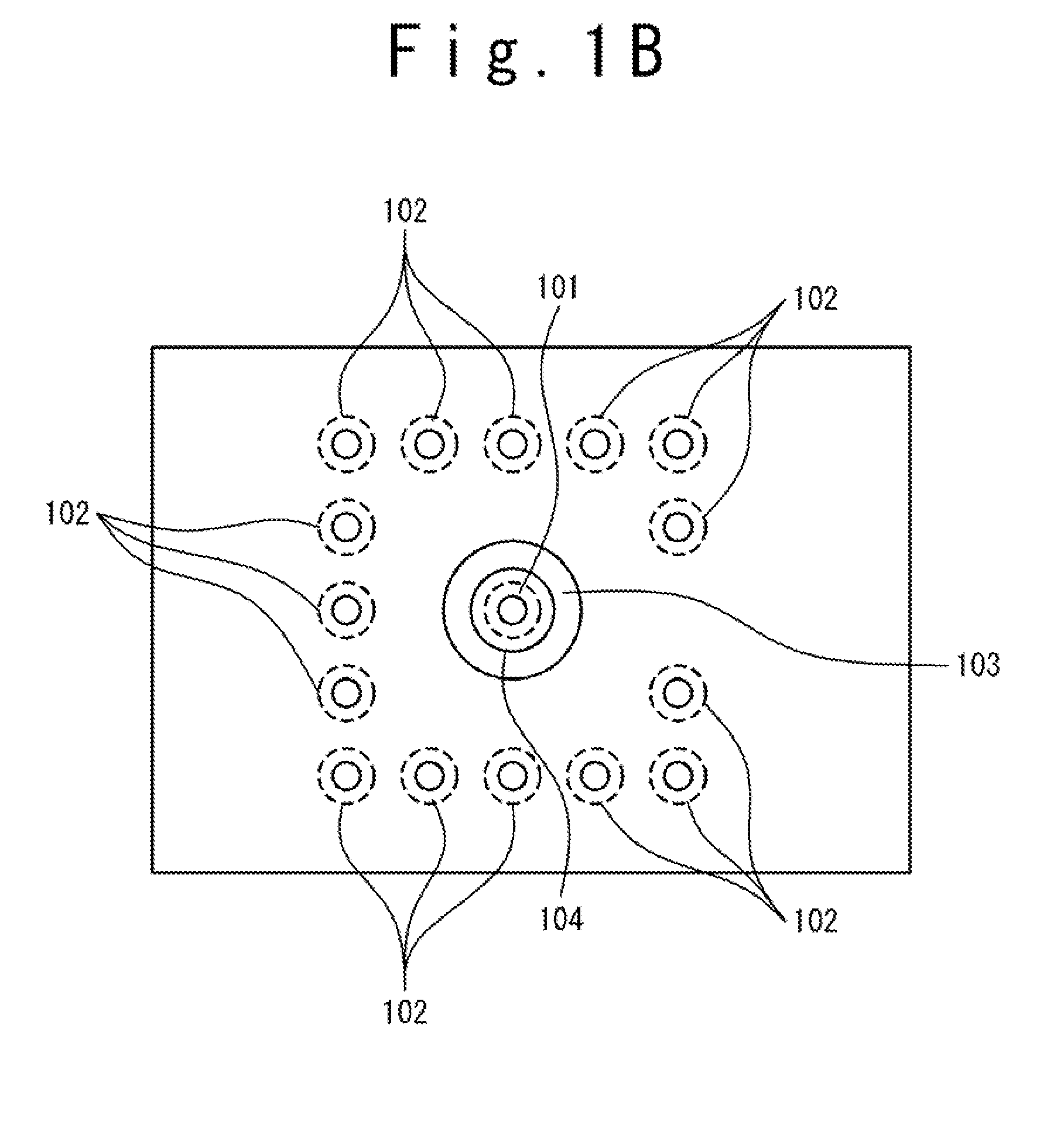
[0065]In FIGS. 1A to 1E, an exemplary embodiment of a combined via structure in a multilayer board is shown. This multilayer board is provided with a plurality of conductor layers 1L1 to 1L6. Six conductor layers 1L1 to 1L6 are isolated by a dielectric material 109. Conductor layers 1L1, 1L2, 1L4, 1L5 and 1L6 serve as ground layers. Conductor layer 1L3 serves as signal transmitting layer.

[0066]Note this six conductor layer board is only an example of multilayer boards and a number of conductor layers, filling material and other board parameters can be different that depends on real applications.

[0067]In present embodiment, the combined via ...


PUM


Abstract

A filter is provided with a planar transmission line and a combined via structure connected to (both) one ends of the planar transmission line. The planar transmission line and the combined via structure are disposed in a same multilayer board. The combined via structure comprises two working parts. The first working part comprises a segment of signal via and a plurality of segments of ground vias surrounding the signal via. The second working part comprises a segment of the same signal via, a plurality of segments of the same ground vias, smooth conductive plate and corrugated conductive plate. The smooth conductive plate and the corrugated conductive plate are connected to the signal via. The second working part comprises a segment of the same signal via, a plurality of segments of the same ground vias and corrugated conductive plate. The corrugated conductive plate is connected to the signal via.

Description

TECHNICAL FIELD [0001]The present invention relates to via structures, formed in multilayer boards, and filtering components, based on the combined via structures.BACKGROUND ART [0002]Next generation networking and computing systems need compact and cost-effective devices to be promoted to the market. At microwave and higher frequencies, distributed-element filters and other devices are necessary. As a cost-effective approach, multilayer board technologies can be applied to design such devices. These technologies can realize a three-dimensional design concept and, as a result, improve compactness of elements forming the systems.[0003]One type of structures, being used as a building block in distributed-element components, is resonant open-circuited and short-circuited stubs which are applied to design the components. Usually, these stubs in multilayer boards are formed as open-circuited or short-circuited planar transmission line segments. In this case, parasitic coupling, unwanted ...

Claims


Application Information

Patent Timeline
IPC IPC(8): H01P1/203
CPCH01P1/2056H01P7/04H05K1/0222H05K1/0251H05K1/116H01P7/08H05K2201/09454H05K2201/09618H05K2201/09627H05K2201/09718H01P1/203H05K3/429
Inventor KUSHTA, TARAS
Owner NEC CORP
Why Eureka
Try Eureka