Liquid crystal display device and method for driving the same

a liquid crystal display and display device technology, applied in the direction of digital storage, instruments, computing, etc., can solve the problems of difficult to improve the characteristics of transistors or the like, and achieve the effect of increasing the frequency of input of an image signal to each pixel

Inactive Publication Date: 2011-10-13
SEMICON ENERGY LAB CO LTD
View PDF22 Cites 38 Cited by
  • Summary
  • Abstract
  • Description
  • Claims
  • Application Information

AI Technical Summary

Benefits of technology

[0008]In view of the above, an object of one embodiment of the present invention is to increase the frequency of input of image signals.
[0013]Note that in a liquid crystal display device, AC voltage is applied to a liquid crystal element provided in a pixel in order to prevent deterioration of liquid crystal (called burn-in). For that reason, a transistor used in a pixel portion preferably has a withstand voltage higher than or equal to about ten and several volts. Moreover, the off-state current of the transistor needs to be low in order to maintain a voltage held at the liquid crystal element. In contrast, for a transistor used in a signal line driver circuit, high-speed operation is more important than high withstand voltage in order to keep high quality of images displayed in the liquid crystal display device.
[0014]In view of the above, a transistor including a channel formation region formed using an oxide semiconductor is used in a pixel portion in a liquid crystal display device according to one embodiment of the present invention. The bandgap of the oxide semiconductor is 3.0 eV to 3.5 eV, which is about three times that of silicon. The wide band gap of the oxide semiconductor is advantageous in increasing the withstand voltage of the transistor. In addition, an oxide semiconductor that is purified by reduction in concentration of impurities such as moisture or hydrogen, which serves as electron donors (donors), that is, a purified OS is an intrinsic semiconductor (an i-type semiconductor) or a substantially intrinsic semiconductor. Therefore, a transistor including the purified oxide semiconductor has very low off-state current in addition to high withstand voltage.
[0015]Furthermore, in the liquid crystal display device according to one embodiment of the present invention, a transistor including a crystalline semiconductor such as polycrystalline or single crystal silicon or polycrystalline or single crystal germanium is used in a driver circuit that needs to operate at higher speed than the pixel portion, such as a signal line driver circuit. The crystalline semiconductor has higher mobility than the oxide semiconductor. Accordingly, a signal line driver circuit can operate at high speed by using the crystalline semiconductor for a transistor.
[0021]In the liquid crystal display device according to one embodiment of the present invention, image signals can be concurrently supplied to pixels placed in a plurality of rows among pixels arranged in matrix. Thus, the frequency of input of an image signal to each pixel can be increased without change in response speed of a transistor or the like included in the liquid crystal display device.

Problems solved by technology

However, it is not easy to improve characteristics of the transistor or the like.

Method used


Image

  • Liquid crystal display device and method for driving the same
  • Liquid crystal display device and method for driving the same
  • Liquid crystal display device and method for driving the same

Examples


embodiment 1

[0049]In this embodiment, an example of a liquid crystal display device in which images are displayed by a field sequential method will be described with reference to FIGS. 1A and 1B, FIG. 2, FIG. 3, FIGS. 4A and 4B, and FIG. 5.

(Structural Example of Liquid Crystal Display Device)

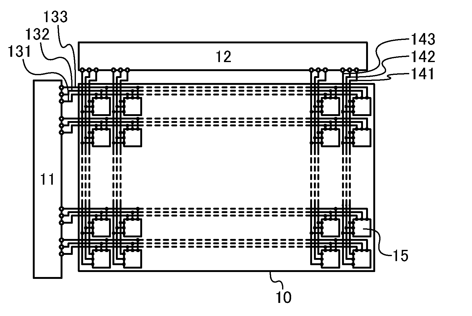
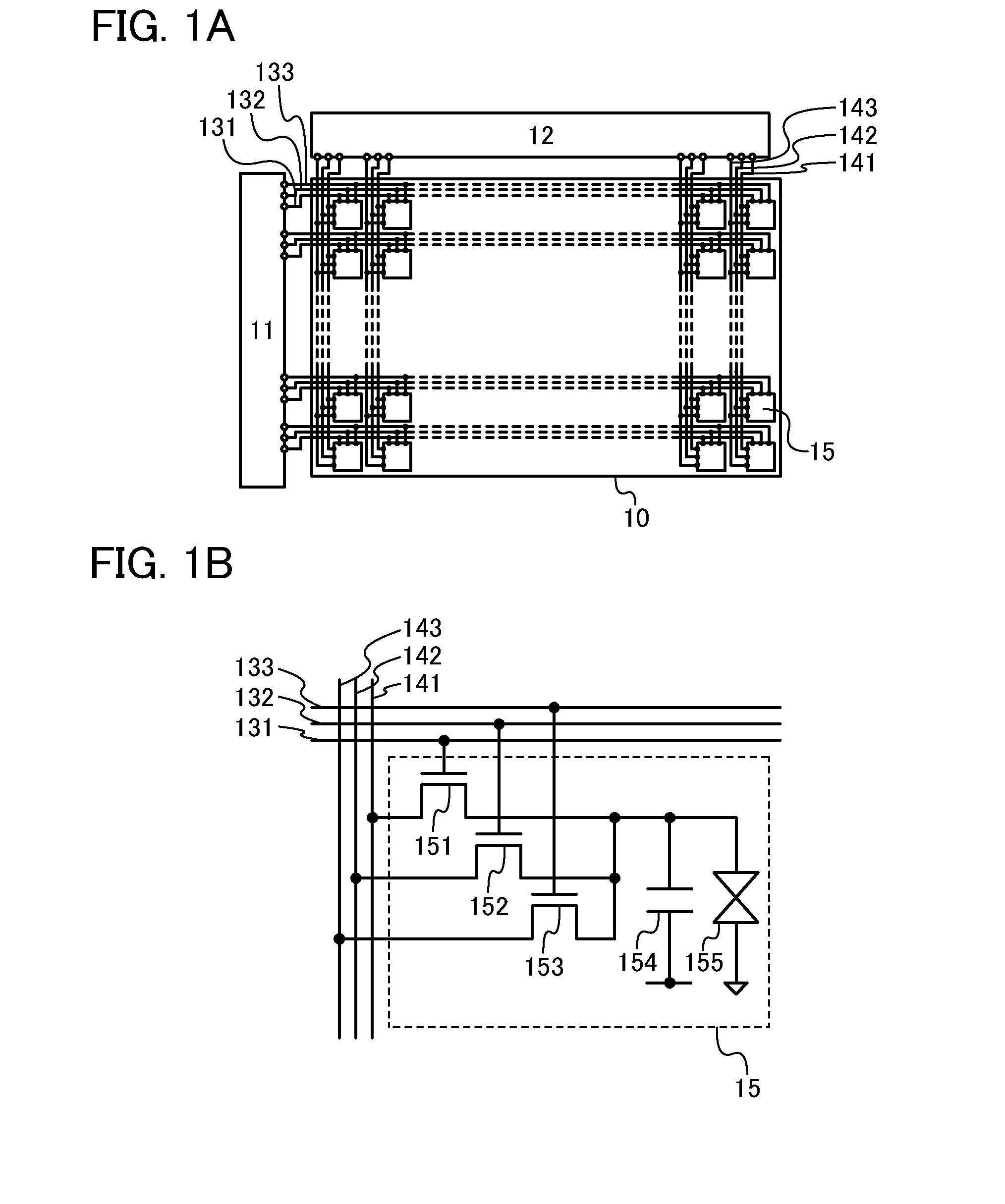
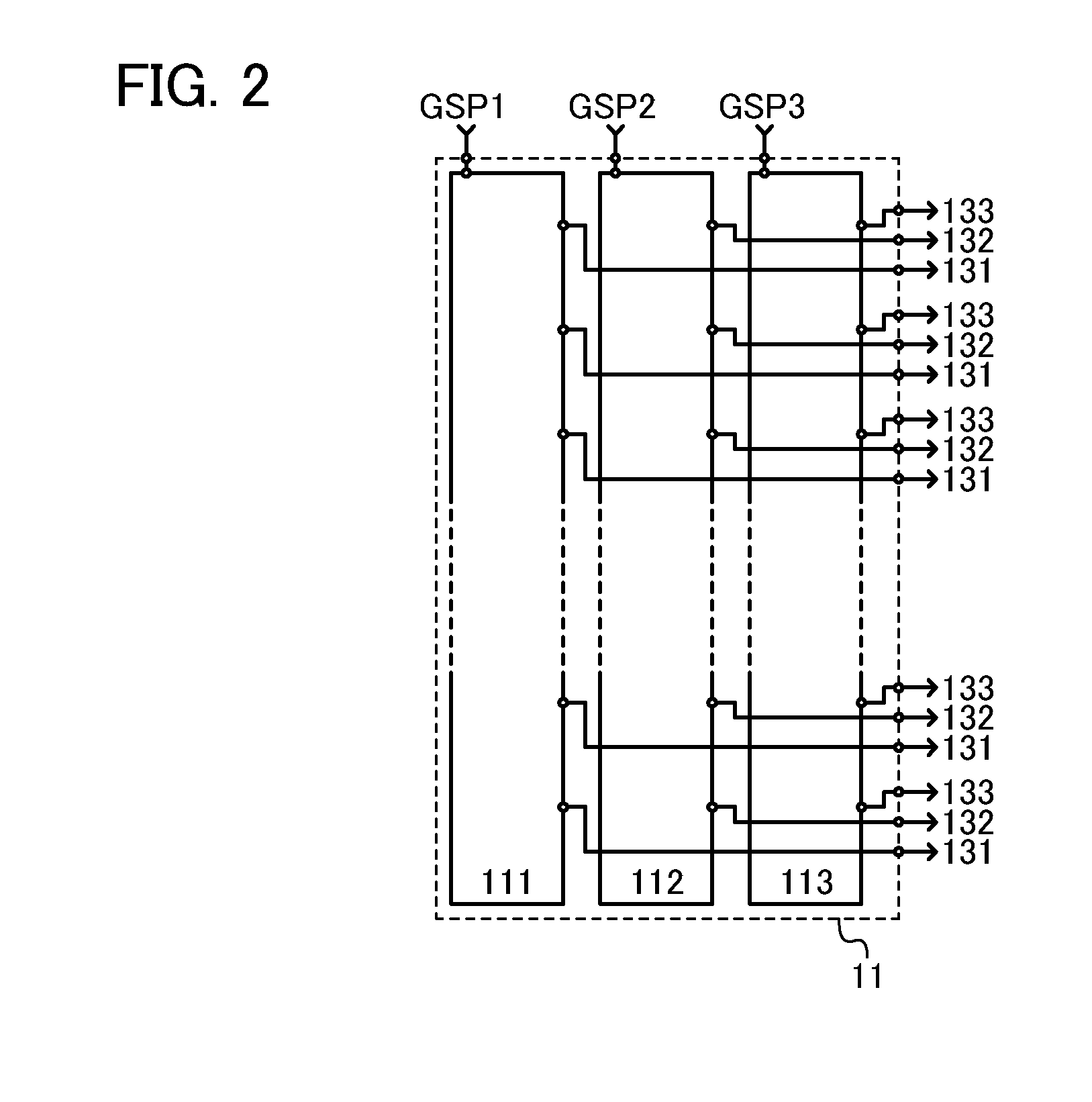
[0050]FIG. 1A illustrates a structural example of a liquid crystal display device. The liquid crystal display device in FIG. 1A includes a pixel portion 10; a scan line driver circuit 11; a signal line driver circuit 12; 3n scan lines 131, 3n scan lines 132, and 3n scan lines 133 (n is a natural number of 2 or more) arranged parallel or approximately parallel to each other; and m signal lines 141, m signal lines 142, and m signal lines 143 (m is a natural number of 2 or more) arranged parallel or approximately parallel to each other. The potentials of the scan lines 131, 132, and 133 are controlled by the scan line driver circuit 11. The potentials of the signal lines 141, 142, and 143 are controlled by the...

embodiment 2

[0073]In this embodiment, an example of a field-sequential liquid crystal display device having a structure different from that in Embodiment 1 will be described with reference to FIGS. 6A to 6D, FIGS. 7A and 7B, and FIG. 8.

(Structural Example of Liquid Crystal Display Device)

[0074]FIG. 6A illustrates a structural example of a liquid crystal display device. The liquid crystal display device in FIG. 6A includes a pixel portion 30; a scan line driver circuit 31; a signal line driver circuit 32; 3n scan lines 33 (n is a natural number of 2 or more) arranged parallel or approximately parallel to each other; and m signal lines 341, m signal lines 342, and m signal lines 343 (m is a natural number of 2 or more) arranged parallel or approximately parallel to each other. The potentials of the scan lines 33 are controlled by the scan line driver circuit 31. The potentials of the signal lines 341, 342, and 343 are controlled by the signal line driver circuit 32.

[0075]The pixel portion 30 is d...

embodiment 3

[0092]In this embodiment, a specific structure of the liquid crystal display device described in Embodiment 1 or 2 will be described.

(Example of Transistor Provided in Pixel)

[0093]In the liquid crystal display device in Embodiment 1, a plurality of transistors are provided in each pixel. Input of an image signal to the pixel is controlled by sequentially using the plurality of transistors. Thus, image signals can be concurrently supplied to pixels placed in a plurality of rows. Note that in the liquid crystal display device, the leakage of an image signal held at a pixel is accordingly increased in accordance with the increase in the number of transistors provided in the pixel. For that reason, in the liquid crystal display device, a transistor with excellent off-state characteristics (with low off-state current) is preferably used as the transistor provided in each pixel. An example of a transistor that is suitable for the transistor will be described below with reference to FIG. 9...


PUM


Abstract

To increase the frequency of input of image signals in terms of design in a field-sequential liquid crystal display device. Image signals are concurrently supplied to pixels provided in a plurality of rows among pixels arranged in matrix in a pixel portion of the liquid crystal display device. Thus, the frequency of input of an image signal to each pixel can be increased without change in response speed of a transistor or the like included in the liquid crystal display device.

Description

TECHNICAL FIELD[0001]The present invention relates to a liquid crystal display device and a method for driving the liquid crystal display device. In particular, the present invention relates to a liquid crystal display device in which images are displayed by a field sequential method, and a method for driving the liquid crystal display device.BACKGROUND ART[0002]A color filter method and a field sequential method are known as display methods for liquid crystal display devices. In a liquid crystal display device in which images are displayed by a color filter method, a plurality of subpixels each having a color filter that transmits only light with a wavelength of a given color (e.g., red (R), green (G), or blue (B)) are provided in each pixel. A desired color is produced in such a manner that transmission of white light is controlled in each subpixel and a plurality of colors are mixed in each pixel. On the other hand, in a liquid crystal display device in which images are displayed...

Claims


Application Information

Patent Timeline
Patent Type & Authority Applications(United States)
IPC IPC(8): G09G3/36G06F3/038
CPCG06F3/0412G09G2310/0286G06F3/045G09G3/006G09G3/3413G09G3/3426G09G3/3648G09G2300/0408G09G2300/0426G09G2310/0235G02F1/13624G02F1/136286G09G3/3674G09G2300/08G06F3/044G06F3/0443G09G3/36G09G3/3655G09G3/3696G09G2320/041G09G2320/103G09G2330/021G09G2340/0435G11C19/28G09G5/18
Inventor KOYAMA, JUNMIYAKE, HIROYUKIYAMAZAKI, SHUNPEI
Owner SEMICON ENERGY LAB CO LTD
Why Eureka
Try Eureka