Display device having parabolic light reflecting portions for enhanced extraction of light

a technology of parabolic light and light-emitting devices, which is applied in the direction of discharge tubes/lamp details, discharge tubes luminescnet screens, electric discharge lamps, etc., can solve the problems of significant power consumption loss, achieve the effect of improving light output efficiency, reducing power consumption, and increasing light output efficiency

Active Publication Date: 2011-10-20
SONY CORP
View PDF6 Cites 8 Cited by
  • Summary
  • Abstract
  • Description
  • Claims
  • Application Information

AI Technical Summary

Benefits of technology

[0006]According to Patent Documents 1, 2 and 3, a reduction in power consumption can be achieved by making effective use of light which would otherwise be wasted through total reflection in a light-emitting device. These patent documents, however, make no mention about optical conditions for an organic EL device, specifically, the optimization of an organic layer, which includes a light-emitting layer, in an organic EL device for the improvement of light outputting efficiency. According to Patent Documents 4 and 5, on the other hand, the efficiency of light output can be increased by introducing a resonator structure. There is, however, an outstanding strong demand for a further improvement in the efficiency of light output.
[0007]It is desirable to provide a display device equipped with a resonator structure and having a structure or construction that makes it possible to achieve a still further improvement in the efficiency of light output.
[0042]When constructed as described immediately above, it is possible to achieve an improvement in brightness within an effective visual range, and therefore, to obtain a bright screen while assuring a still further reduction in the power consumption of the display device.
[0067]The display device according to the first embodiment or second embodiment of the present invention can be constructed in an embodiment that the first electrode is formed of a light reflecting material, the second electrode is formed of a semi-transparent material, and m1=0 and m2=1 which can make highest the efficiency of light output. In the display device according to the first embodiment or second embodiment of the present invention or the display device according to the fifth embodiment of the present invention to be described subsequently herein, electrons can be supplied in a quantity necessary and sufficient for higher efficiency to the light-emitting layer efficiently at a low drive voltage by making an electron transport layer (electron supply layer) thicker than a hole transport layer (hole support layer). Described specifically, the supply of holes can be increased by arranging the hole transport layer between the first electrode, which corresponds to an anode electrode, and the light-emitting layer and forming the hole transport layer with a thickness smaller than the electron transport layer. This construction makes it possible to obtain a carrier balance with neither too much nor too little holes or electrons and with a sufficiently large carrier supply, and therefore, to obtain a high efficiency of light emission. Because holes and electrons are neither too much nor too little, the carrier balance is resistant to disruption, a drive deterioration is reduced, and the light-emitting life can be prolonged.
[0084]The display device according to the third embodiment or fourth embodiment of the present invention can be constructed in an embodiment that the first electrode is formed of a semi-transparent material, the second electrode is formed of a light reflecting material, and m1=1 and m2=2 which can make highest the efficiency of light output. In the display device according to the third embodiment or fourth embodiment of the present invention, necessary and sufficient electrons can also be supplied in a quantity necessary and sufficient for higher efficiency to the light-emitting layer at a low drive voltage by making an electron transport layer thicker than a hole transport layer. Described specifically, the supply of holes can be increased by arranging the hole transport layer between the second electrode, which corresponds to an anode electrode, and the light-emitting layer and forming the hole transport layer with a thickness smaller than the electron transport layer. This construction makes it possible to obtain a carrier balance with neither too much nor too little holes or electrons and with a sufficiently large carrier supply, and therefore, to obtain a high efficiency of light emission. Because holes and electrons are neither too much nor too little, the carrier balance is resistant to disruption, a drive deterioration is reduced, and the light-emitting life can be prolonged.
[0100]The display device according to the fifth embodiment of the present invention, which may include one or more of the above-described preferred embodiments, can be constructed in an embodiment that the first electrode is formed of a light reflecting material, the second electrode is formed of a semi-transparent material, and m1=0 and m2=1 which can make highest the efficiency of light output.

Problems solved by technology

Concerning organic EL display devices, there is a strong demand for the development of a technology that makes it possible to realize an efficient output of light, because a low light output efficiency means ineffective utilization of an actual luminous quantity in an organic EL device and becomes a cause of a significant loss in power consumption or the like.

Method used


Image

  • Display device having parabolic light reflecting portions for enhanced extraction of light
  • Display device having parabolic light reflecting portions for enhanced extraction of light
  • Display device having parabolic light reflecting portions for enhanced extraction of light

Examples


example 1

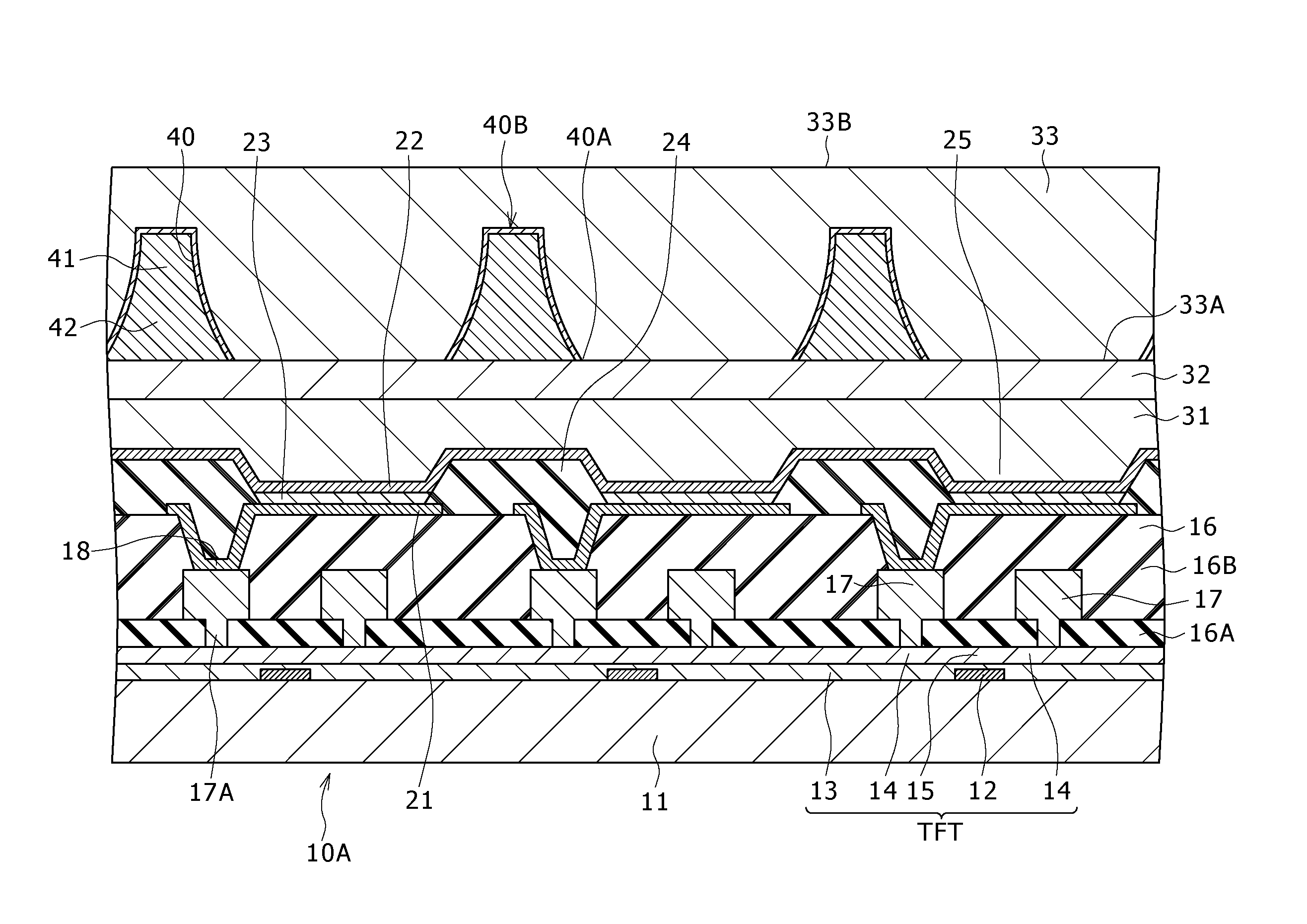
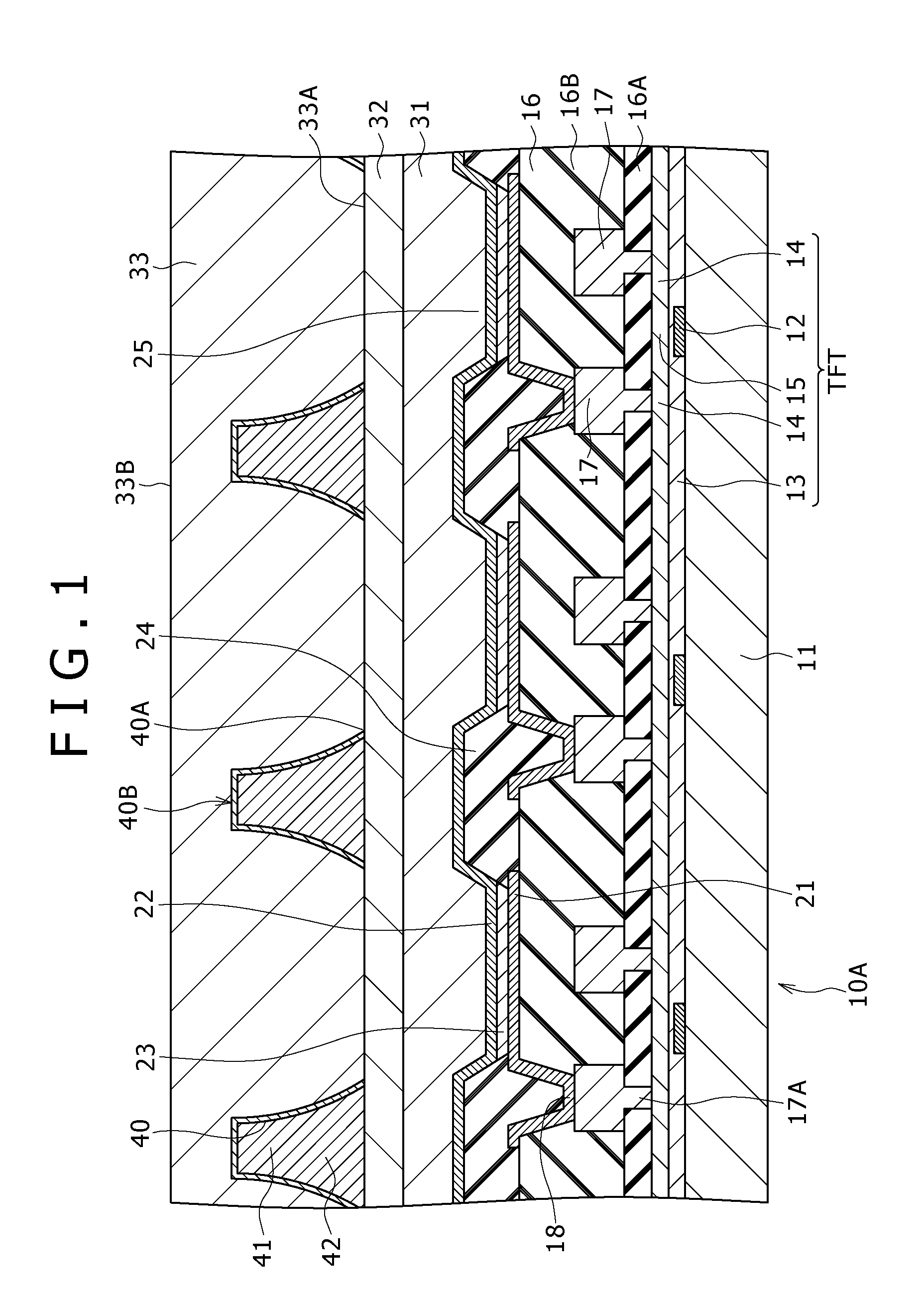
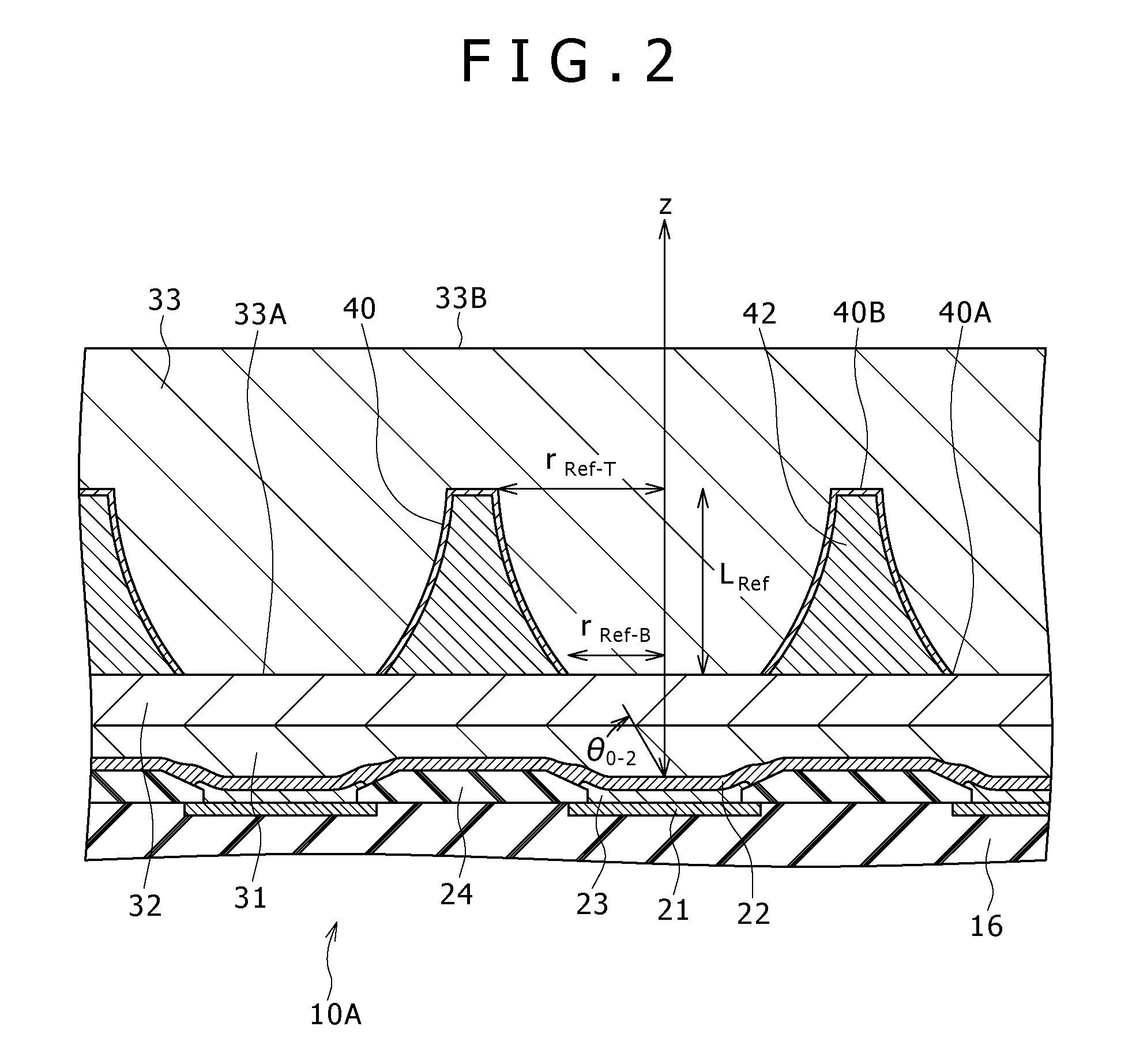
[0133]Example 1 relates to a display device with which the first embodiment and fifth embodiment of the present invention are concerned, and specifically to an organic EL display device. The display device (which may hereinafter be called “the organic EL display device) of Example 1 is shown, as a schematic fragmentary cross-sectional view, in FIG. 1, a schematic view of its light reflecting portions is depicted in FIG. 2, and a schematic view of its organic layers and the like is illustrated in FIG. 3A. The organic EL display device of Example 1 is an organic EL color display device of the active matrix type, and is of the surface-emitting type. Namely, light is outputted through a second electrode which corresponds to an upper electrode.

[0134]The organic EL display device of Example 1 and the below-described organic EL display devices of Examples 2 to 4 are each provided with a plurality (for example, N×M=2,880×540) of light-emitting devices (specifically, organic EL devices) 10A....

example 2

[0207]Example 2 relates to a display device with which the second embodiment and fifth embodiment of the present invention are concerned, and specifically to an organic EL display device. The organic EL display device of Example 2 is shown, as a schematic fragmentary cross-sectional view, in FIG. 6, and a schematic fragmentary cross-sectional view of its lens portions is depicted in FIG. 7. A concept diagram of an organic layer is similar to that illustrated in FIG. 3A. The organic EL display device of Example 2 is also an organic EL color display device of the active matrix type, and is also of the surface-emitting type. Namely, light is outputted through a second electrode which corresponds to an upper electrode.

[0208]In the organic EL display device of Example 2, lens portions 50 are formed on the first side 33A of the transparent upper substrate 33 such that light, which is extracted from the light-emitting layer 23A through the second electrode 22, is allowed to pass through th...

example 3

[0214]Example 3 relates to a display device with which the third embodiment of the present invention is concerned, and specifically to an organic EL display device. A schematic fragmentary cross-sectional view of the organic EL display device of Example 3 is shown in FIG. 8, and a schematic fragmentary cross-sectional view of its organic layer and the like is depicted in FIG. 9. The organic EL display device of Example 3 is also an organic EL color display device of the active matrix type, but is of the bottom-emitting type. Namely, light is outputted through a first electrode which corresponds to a lower electrode.

[0215]The organic EL display device of Example 3 or of Example 4 to be described subsequently herein is provided with:

[0216](A) a transparent lower substrate having a first side 11A and a second side 11B located on an opposite side of the first side 11A (in Example 3, a first substrate 11 also serves as the transparent lower substrate), and

[0217](B) a plurality of light-e...


PUM


Abstract

Disclosed herein is a display device provided with: (A) a plurality of light-emitting devices comprising a first electrode, an organic layer including a light-emitting layer and a second electrode configured to resonate light, which is generated in the light-emitting layer, between a first interface defined by an interface between the first electrode and the organic layer and a second interface defined by an interface between the second electrode and the organic layer, and (B) a transparent upper substrate having a first side facing the second electrode and a second side located on an opposite side of the first side, and fixed above the second electrode.

Description

CROSS REFERENCES TO RELATED APPLICATIONS[0001]This application is a divisional application of U.S. patent application Ser. No. 12 / 190,858, filed Aug. 13, 2008, the entirety of which is incorporated herein by reference to the extent permitted by law. The present application also claims priority to Japanese Patent Application JP 2007-212956 filed in the Japan Patent Office on Aug. 17, 2007, the entire contents of which being incorporated herein by reference.BACKGROUND OF THE INVENTION[0002]This invention relates to a display device, and more specifically, to a display device equipped with light-emitting devices having a resonator structure.[0003]In recent years, lighting devices and organic electroluminescence display devices (hereinafter simply called “organic EL display devices”) making use of organic electroluminescence devices (hereinafter simply called “organic EL devices”) are finding widespread utility. Concerning organic EL display devices, there is a strong demand for the dev...

Claims


Application Information

Patent Timeline
Patent Type & Authority Applications(United States)
IPC IPC(8): H01J1/62
CPCH01L51/5265H01L51/5275H01L51/5271Y02E10/549H10K50/852H10K50/856H10K50/858H01L29/66439H01L2924/2024H10K30/82
Inventor YAMADA, JIROKASHIWABARA, MITSUHIROFUKUDA, TOSHIHIROASAKI, REOKANO, GENTARO
Owner SONY CORP
Why Eureka
Try Eureka