
Method for manufacturing LED package and substrate thereof

a technology of led package and substrate, which is applied in the direction of semiconductor/solid-state device manufacturing, semiconductor devices, electrical devices, etc., can solve the problems of reduced life and light efficiency of led, complicated method for manufacturing substrate, and limited thermal dissipation of led packag

Inactive Publication Date: 2011-10-20
ADVANCED OPTOELECTRONICS TECH
View PDF3 Cites 16 Cited by
  • Summary
  • Abstract
  • Description
  • Claims
  • Application Information

AI Technical Summary

Benefits of technology

[0005]Generally, the LED package comprises a substrate for carrying the LED chip, wherein heat generated from the LED chip is dissipated via the substrate to the exterior. The substrate also includes a circuit formed on the bilateral sides of the substrate by using drilling and numerous electroplating, whereby method for manufacturing the substrate is complicated. Furthermore, while thickness of the circuit is limited to compact size of the LED package, thermal dissipation of the LED package is also restricted.

Problems solved by technology

Besides heat generated from LED results ambient temperature raised that lead to lifetime and light efficiency reduction of the LED.
The substrate also includes a circuit formed on the bilateral sides of the substrate by using drilling and numerous electroplating, whereby method for manufacturing the substrate is complicated.
Furthermore, while thickness of the circuit is limited to compact size of the LED package, thermal dissipation of the LED package is also restricted.

Method used


Image

  • Method for manufacturing LED package and substrate thereof
  • Method for manufacturing LED package and substrate thereof
  • Method for manufacturing LED package and substrate thereof

Examples


Embodiment Construction

[0015]Exemplary embodiments of the disclosure will now be described with reference to the accompanying drawings.

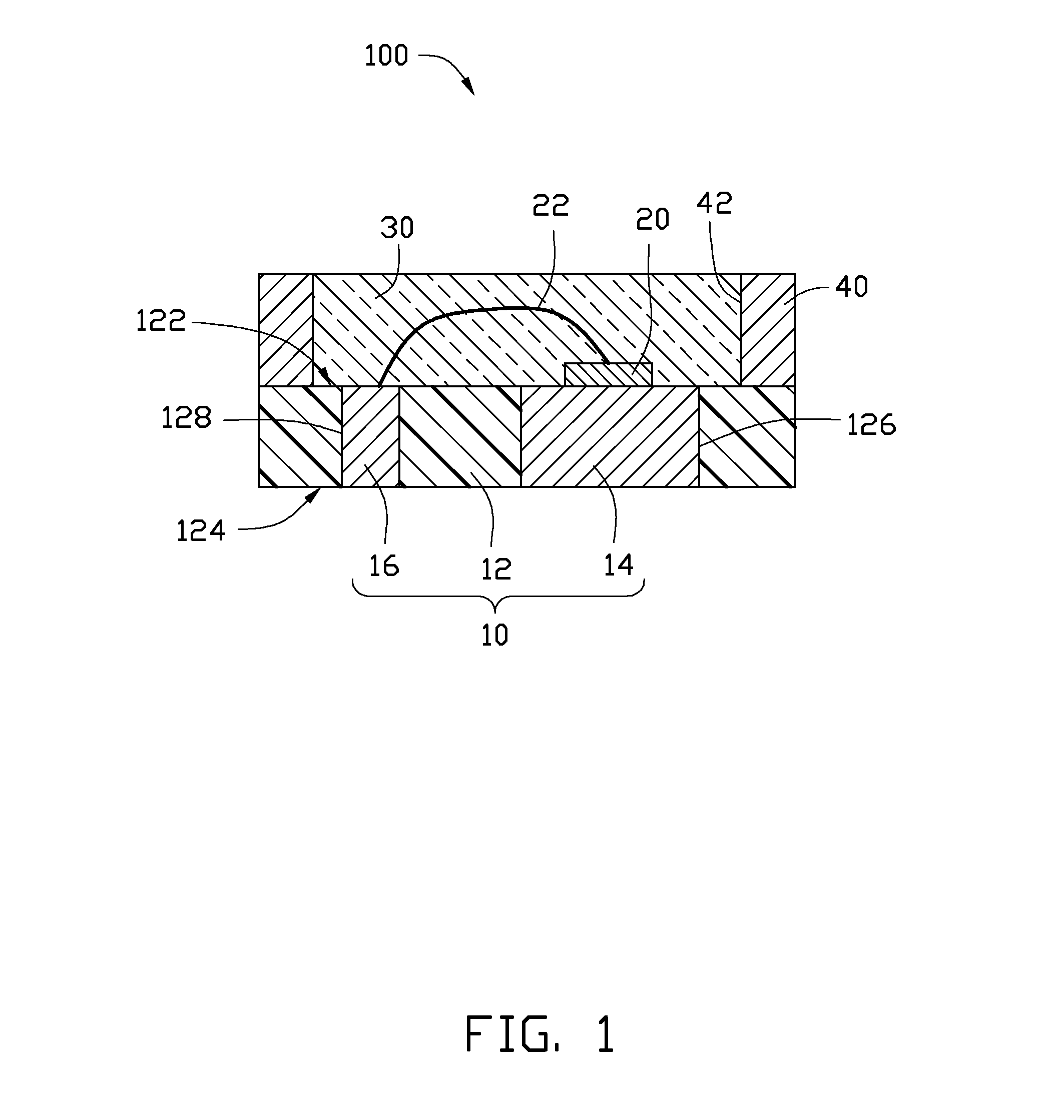
[0016]Referring to FIG. 1, the disclosure provides a first embodiment of a LED package 100 comprising a substrate 10, a LED chip 20, an encapsulation 30 and a reflector 40.

[0017]The substrate 10 comprises an insulator 12, a first electrode 14 and a second electrode 16. The insulator 12 includes a first surface 122 and a second surface 124 opposite to the first surface 122, wherein a first through hole 126 and a second through hole 128 pass through the insulator 12 from the first surface 122 to the second surface 124. The insulator 12 is thermally conductive and electrically insulating material such as epoxy, silicone, silicon oxide or a mixture thereof. The first electrode 14 and the second electrode 16 are respectively allocated inside the first through hole 126 and the second through hole 128. The first electrode 14 and the second electrode 16 are even with the insulator...


PUM


Abstract

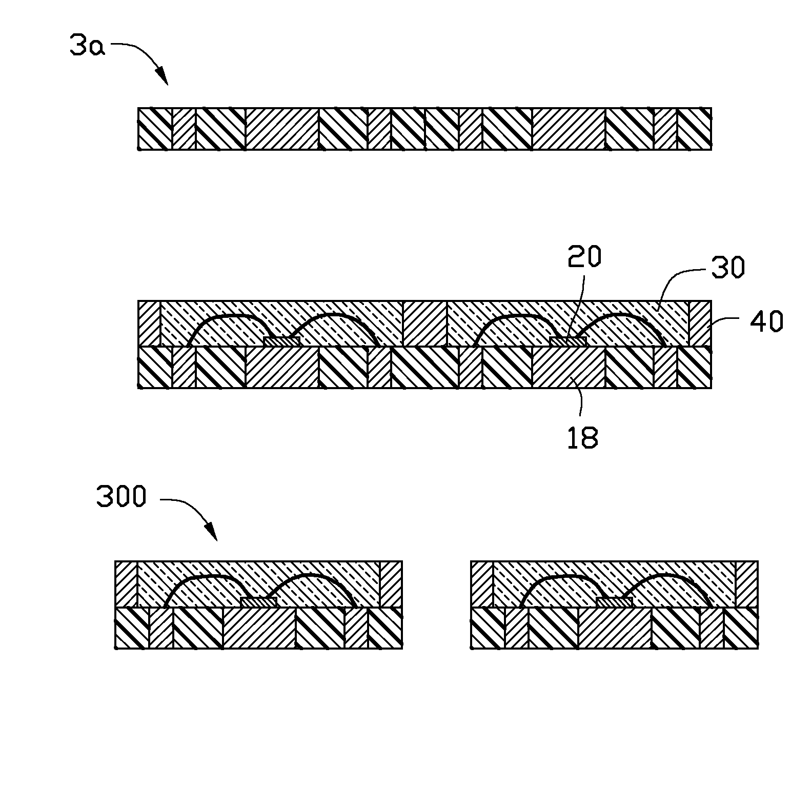
In a method for manufacturing a LED package, a substrate of the LED package is formed by thermally pressing at least one insulating plate over an electrode plate and then grinding the insulating plates to expose the electrode plate.

Description

BACKGROUND[0001]1. Technical Field[0002]The disclosure relates generally to semiconductor package technology, and more particularly to a method for manufacturing LED package and substrate thereof.[0003]2. Description of the Related Art[0004]Light emitting diodes (LED) are widely applied to many technical fields due to longer lifetime, lower power consumption, less heat generation, and compact size. Specifically, the LED is capable of emitting light of varied wavelengths, although most capable energy of the LED is transformed into heat and only the remained energy is transformed into light emitted. Besides heat generated from LED results ambient temperature raised that lead to lifetime and light efficiency reduction of the LED. Hence efficient thermal-dissipation is very critical for the LED packages.[0005]Generally, the LED package comprises a substrate for carrying the LED chip, wherein heat generated from the LED chip is dissipated via the substrate to the exterior. The substrate ...

Claims


Application Information

Patent Timeline
Patent Type & Authority Applications(United States)
IPC IPC(8): H01L33/48
CPCH01L24/97H01L2924/12041H01L33/647H01L2224/48091H01L2224/97H01L2924/01013H01L2924/01029H01L2924/01047H01L2924/01049H01L2924/01079H01L2924/01082H01L33/48H01L2924/01065H01L2924/01033H01L2924/01006H01L2924/00014H01L2224/85
Inventor LIN, SHEN-BO
Owner ADVANCED OPTOELECTRONICS TECH
Learn More