Solid imaging apparatus
a technology of solid imaging and apparatus, applied in the field of solid imaging apparatus, can solve the problem that the maximum amplitude of the 0-degree phase cannot be effectively utilized to reduce the resolution, and achieve the effect of less jitter
- Summary
- Abstract
- Description
- Claims
- Application Information
AI Technical Summary
Benefits of technology
Problems solved by technology
Method used
Image
Examples
embodiment 1
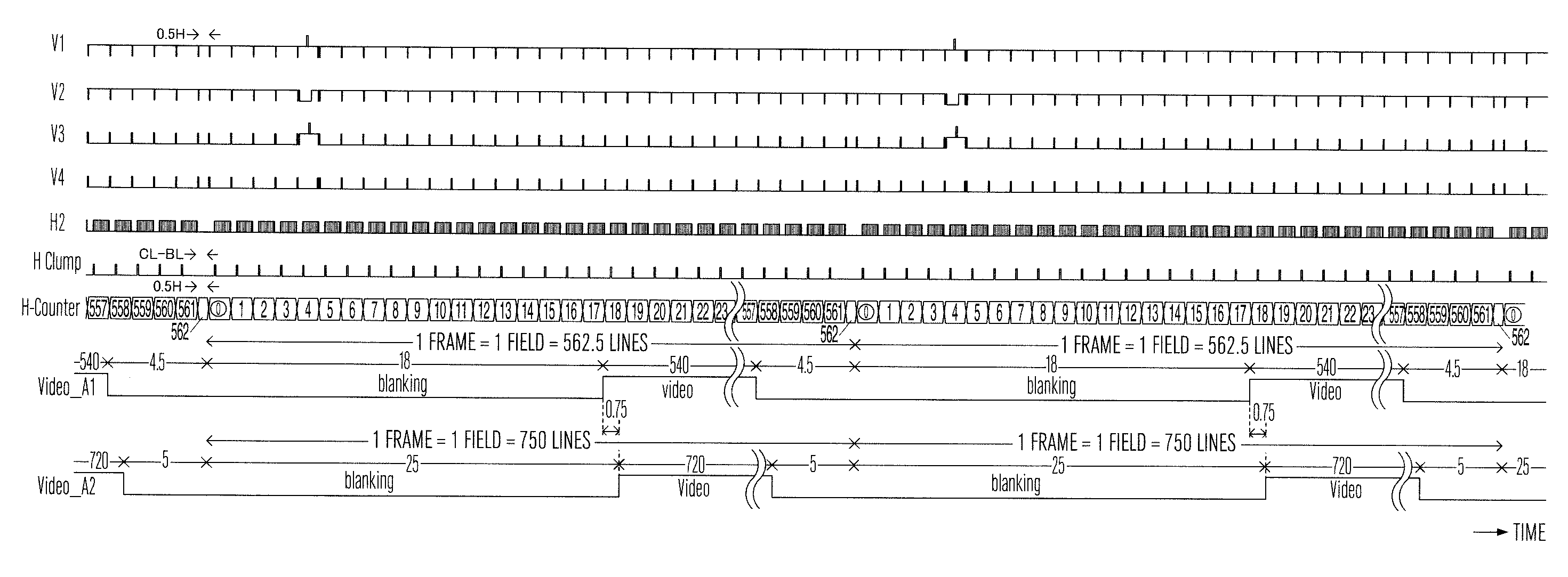
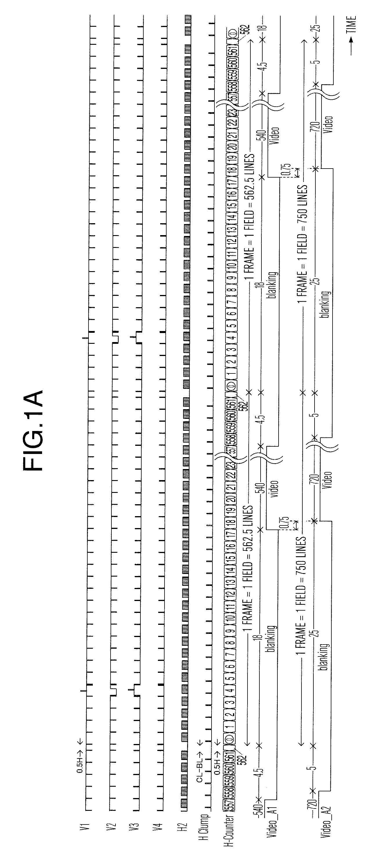
[0072]Referring now to FIG. 1A of a timing chart showing operation an imaging apparatus according to an embodiment of the present invention and FIG. 2 showing a schematic diagram illustrating vertical pixel addition operation of the imaging apparatus of the embodiment of the present invention, the embodiment of the present invention is described.
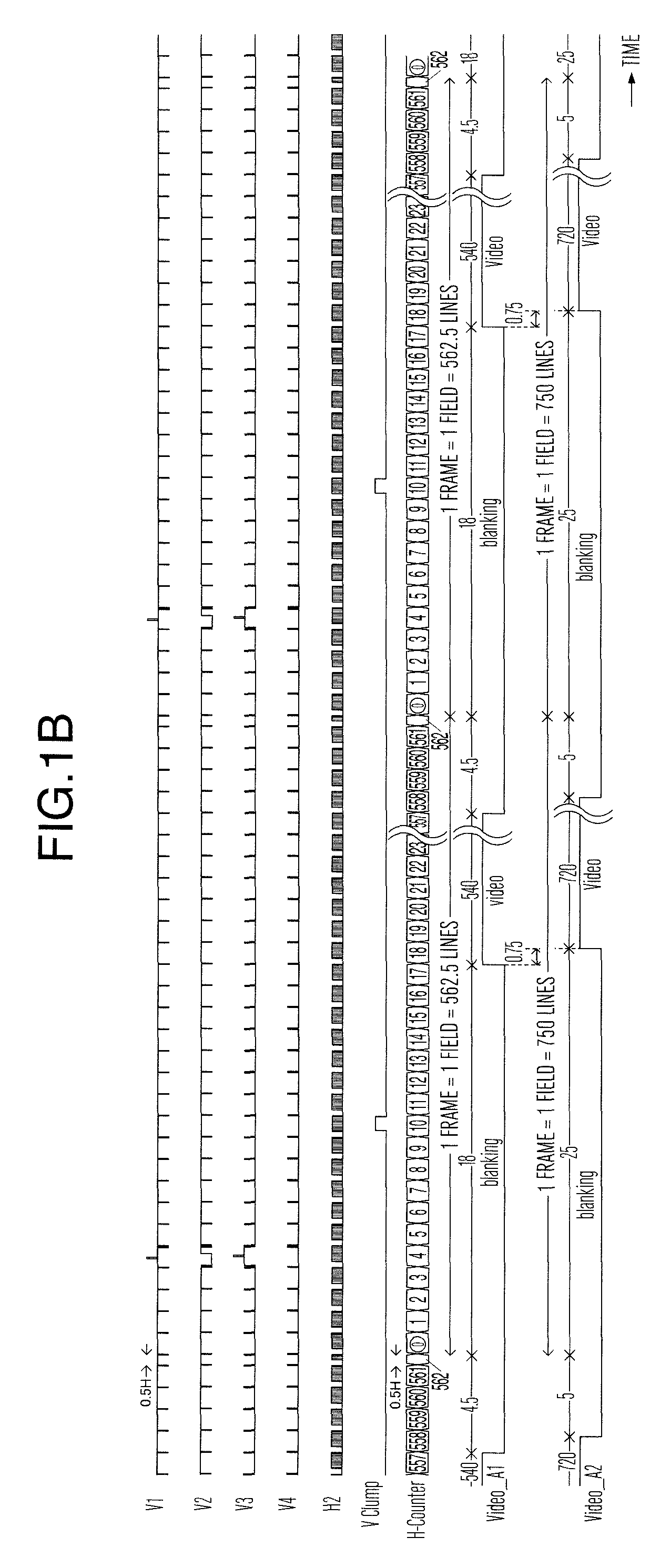
[0073]Referring together to FIG. 1B of a timing chart showing operation of an imaging apparatus according to another embodiment of the present invention, difference of measures different from FIG. 1A is described.
[0074]In FIG. 1A of the timing chart showing operation of the imaging apparatus according to the embodiment of the present invention, V1-V4 represent operation of reading vertical transfer of vertical transfer paths V1 to V4 in IT-CCD. Concretely, V1 to V4 represent reading of electric charges from PD to V1 and V3, vertical pixel addition using V2 and vertical transfer operation for a set of V1 to V4. In the embodiment, description ...
embodiment 2
[0096]Another embodiment of the present invention is now described with reference to FIG. 3 of a timing chart showing operation of an imaging apparatus according to another embodiment of the present invention and FIGS. 4A, 4B, 4C of a schematic diagram illustrating vertical pixel addition operation of the imaging apparatus according to another embodiment of the present invention.
[0097]In FIG. 3 of the timing chart showing operation of the imaging apparatus according to the embodiment of the present invention, V1 to V4 represent operation of reading vertical transfer of vertical transfer paths V1 to V4 in IT-CCD. Concretely, reading of electric charges from PD to V1 and V3, vertical pixel addition of odd field image using V2 and vertical pixel addition of even field image using V4 and vertical transfer operation for a set of V1 to V4 are shown.
[0098]In FIG. 3, the periods of odd field and even field are different by 1H from each other.
[0099]In FIG. 3, H2 represents operation of horiz...
PUM
 Abstract
Description
Claims
Application Information


