Lamination of electrochromic device to glass substrates

a technology of electrochromic devices and glass substrates, applied in the direction of manufacturing tools, non-linear optics, instruments, etc., can solve the problems of high cost of manufacturing, large stress on glass, and high cost of manufacturing devices based on glass substrates, so as to improve manufacturing efficiency

Active Publication Date: 2011-11-03
SAGE ELECTROCHROMICS
View PDF13 Cites 110 Cited by
  • Summary
  • Abstract
  • Description
  • Claims
  • Application Information

AI Technical Summary

Benefits of technology

[0036]In some embodiments, by withstanding similar stresses it is meant that that the electrochromic device laminates or IGUs of the present invention pass about the same industry standard tests as traditional electrochromic devices or IGUs. In other embodiments, by withstanding similar stresses it is meant that that the electrochromic device laminates or IGUs of the present invention can withstand (i) stresses safely in excess of maximum in-service thermomechanical stresses encountered in traditional EC applications, and / or (ii) at least about 50% of the same service loads or stresses as traditional EC devices or IGUs. Applicants have also surprisingly found that that these objectives can be achieved using annealed glass substrates upon which the electrochromic stack is applied or deposited.
[0037]Applicants have unexpectedly found that the improved methods of manufacturing provide for electrochromic device laminates or IGUs that can withstand service loads or stresses similar to those encountered by ICUs produced by traditional means, while providing enhanced manufacturing efficiency and meeting industry standards.
[0038]Moreover, Applicants have surprisingly discovered that annealed glass substrates can be laser cut to produce a sufficiently defect free edge that will, it is believed, endure the full range of thermal and load stresses that the EC device laminate will be subjected to during its service life. Applicants have tested the laser cut glass and the EC device laminates of FIG. 1B at the high end of the thermal and mechanical stress parameter space and have determined that laser cut, EC device laminates or substrates are highly durable and suitable for use in residential and commercial architectural applications and other applications.
[0039]Moreover, Applicants have found that the “coat-then-cut” and “cut-then-coat-then-cut” processes, both described further herein, allow for coating of large substrate panels and custom sizing after coating. Applicants have also found that this process provides improved process control and better overall uniformity of the film coatings of the EC device. Indeed, it is believed that when glass panels all having about the same dimensions are used, subsequent processing temperatures and sputtering plasma conditions for each and every panel will be about the same. This leads, it is believed, to more efficient, continuous coater or sputter operation without the need to slow or stop production or to make process adjustments for the many glass thicknesses, tints, and sizes desired. Thus, throughput rate and uptime are maximized, resulting in lower, more competitive product costs when manufacturing electrochromic devices or IGUs.

Problems solved by technology

Glass, especially glass that is tinted, is subjected to large stresses due to non-uniform heating caused by the absorption of solar radiation.
These stresses can be so great as to cause fractures or cracks to develop in the glass, which could ultimately lead to failure.
This results in stress, typically along the glass edges, which if greater than about 14 to about 28 MPa, could result in cracking.
Of course, this adds to the cost of manufacturing.
While this is a practical solution, the cost of manufacturing devices based on these substrates is expensive.

Method used


Image

  • Lamination of electrochromic device to glass substrates
  • Lamination of electrochromic device to glass substrates
  • Lamination of electrochromic device to glass substrates

Examples


example 1

EC Laminate

[0100]

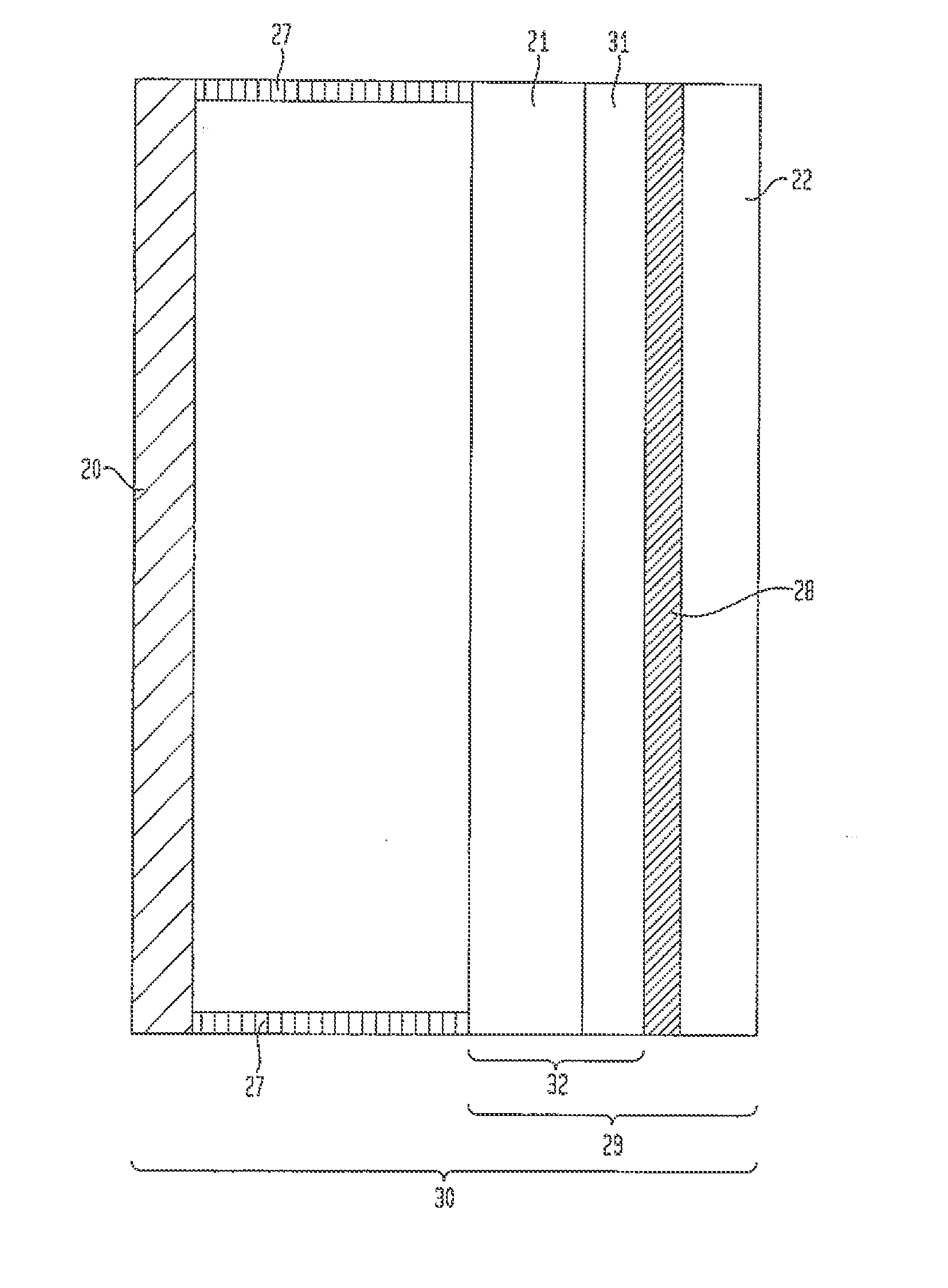
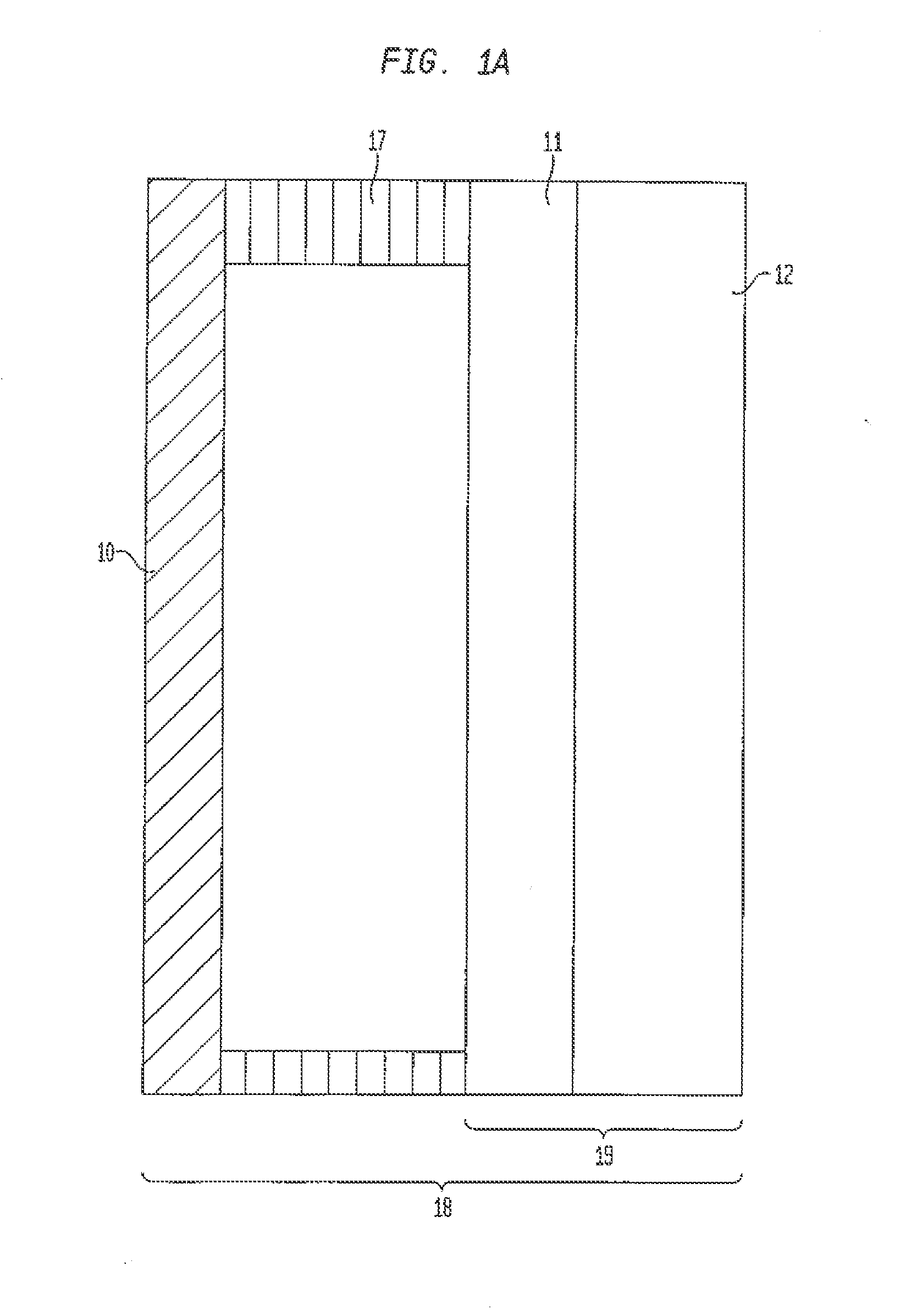
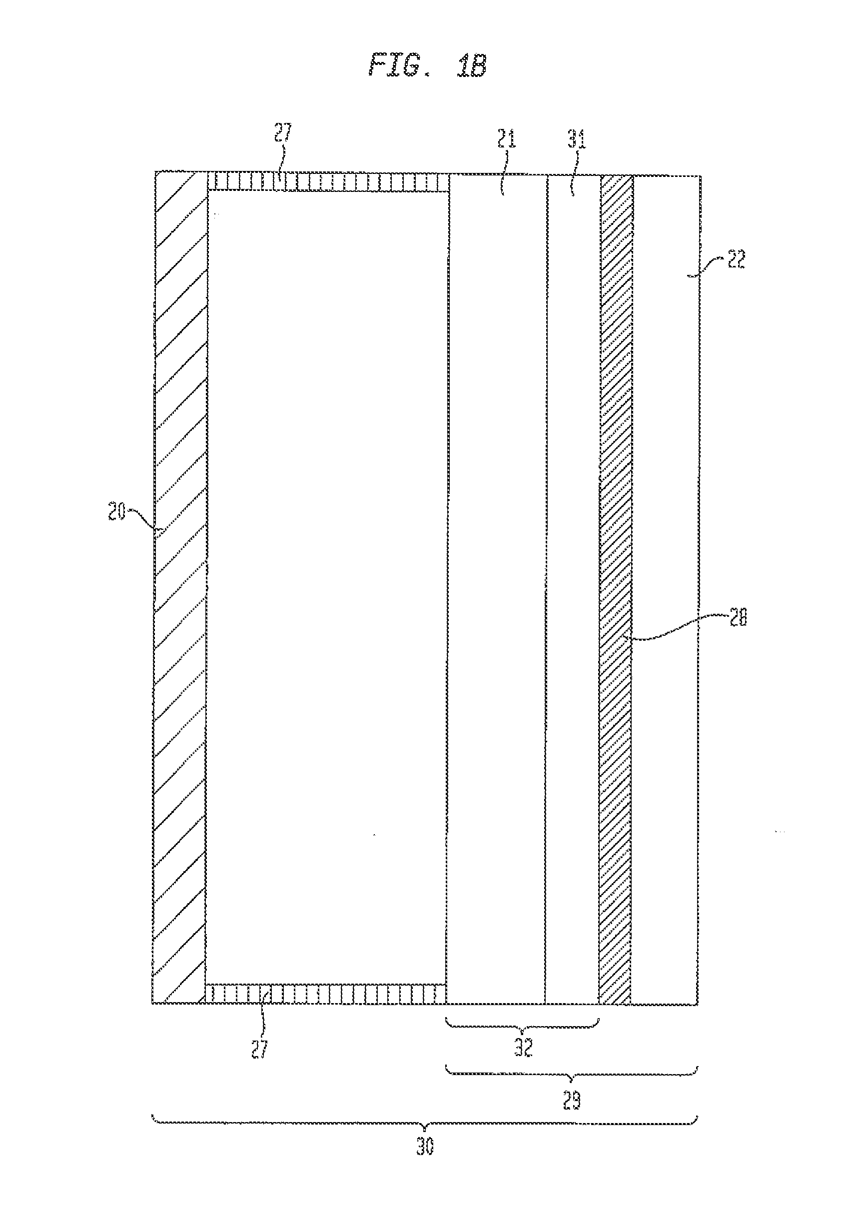
ComponentMaterialProertiesEC outer laminateFully temperedThickness: 3.2 mmglass panesoda-lime glassCTE: 8.5 ppm / KEC substrateAnnealed soda-limeThickness: 1.7 mmfloat glassCTE: 8.5 ppm / NInterlayer materialPVBThickness: 0.76 mm

[0101]Method of Manufacture:

[0102]The laminated EC structure of Example 1 was manufactured according to a “cut-then-coat” process. The lamination was performed using a conventional nip roller / autoclave process. Equivalent results could be obtained using a vacuum, laminating process.

[0103]Results:

[0104]The laminated EC structure having the components detailed above passed the ANSI Z97.1 standard for impact testing.

example 2

EC Laminate

[0105]

ComponentMaterialPropertiesEC outer laminateFully temperedThickness: 4 mmglass panesoda-lime glassCTE: 8.5 ppm / KEC substrateAnnealed soda-limeThickness: 1.7 mmfloat glassCTE: 8.5 ppm / KInterlayer materialPVBThickness: 0.76 mm

[0106]Method of Manufacture

[0107]The laminated EC structure of Example 2 was manufactured according to a “cut-then-coat” process. The lamination was performed using a conventional nip roller / autoclave process.

[0108]Results:

[0109]The laminated EC structure having the components detailed above passed the ANSI Z97.1 standard for impact testing.

[0110]Outer laminate panels having different thicknesses were tested in Examples 1 and 2, with the resulting laminates both passing impact testing. Equivalent results could be obtained using a vacuum laminating process.

example 3

EC Laminate

[0111]

ComponentMaterialPropertiesEC outer laminateFully temperedThickness: 3.2 mmglass panesoda-lime glassCTE: 8.5 ppm / KEC substrateAnnealed soda-limeThickness: 1.7 mmfloat glassCTE: 8.5 ppm / Kinterlayer materialSentryGlas PlusThickness: 0.89 mm(DuPont)

[0112]Method of Manufacture:

[0113]The laminated EC structure of Example 3 was manufactured according to “cut-then-coat” process. The lamination was performed using a conventional nip roller / autoclave process.

[0114]Results:

[0115]The laminated EC structure having the components detailed above passed the ANSI Z97.1 standard for impact testing. Equivalent results could be obtained using a vacuum laminating process.


PUM


Abstract

Electrochromic device laminates and their method of manufacture are disclosed.

Description

CROSS-REFERENCE TO RELATED APPLICATIONS[0001]This application is a continuation, of U.S. application Ser. No. 13 / 040,787, which application claims the benefit of the filing dates of U.S. Provisional Patent Application Nos. 61 / 311,001 filed Mar. 5, 2010 and 61 / 412,153 filed Nov. 10, 2010, the disclosures of which are hereby incorporated herein by reference.BACKGROUND OF THE INVENTION[0002]Glass, especially glass that is tinted, is subjected to large stresses due to non-uniform heating caused by the absorption of solar radiation. These stresses can be so great as to cause fractures or cracks to develop in the glass, which could ultimately lead to failure.[0003]The center of the glass (COG) may have a considerably higher temperature than, for example, the edges of the glass, which are typically covered or shadowed by a frame or other architectural structure. Of course, the more tinted the glass, the greater the solar absorption, and the larger the potential temperature differential bet...

Claims


Application Information

Patent Timeline
Patent Type & Authority Applications(United States)
IPC IPC(8): G02F1/15B32B37/02B32B38/10
CPCB32B17/10045B32B17/10174B32B17/10743B32B17/10761B32B17/10981Y10T156/1062G02F1/1533B32B38/0004G02F1/153G02F1/15Y10T156/1075C03B33/076G02F1/133351Y10T156/1064Y10T156/1052Y10T156/1089B32B17/10513C03B33/0222C03B33/027C03B33/091G02F1/1514
Inventor SBAR, NEIL L.VAN DINE, JOHN E.MCCOY, MICHAEL A.
Owner SAGE ELECTROCHROMICS
Why Eureka
Try Eureka