Resistor and method of forming a resistor
- Summary
- Abstract
- Description
- Claims
- Application Information
AI Technical Summary
Benefits of technology
Problems solved by technology
Method used
Image
Examples
Embodiment Construction
[0019]Hereinafter, some embodiments of the present invention will be described with reference to the accompanying drawings.
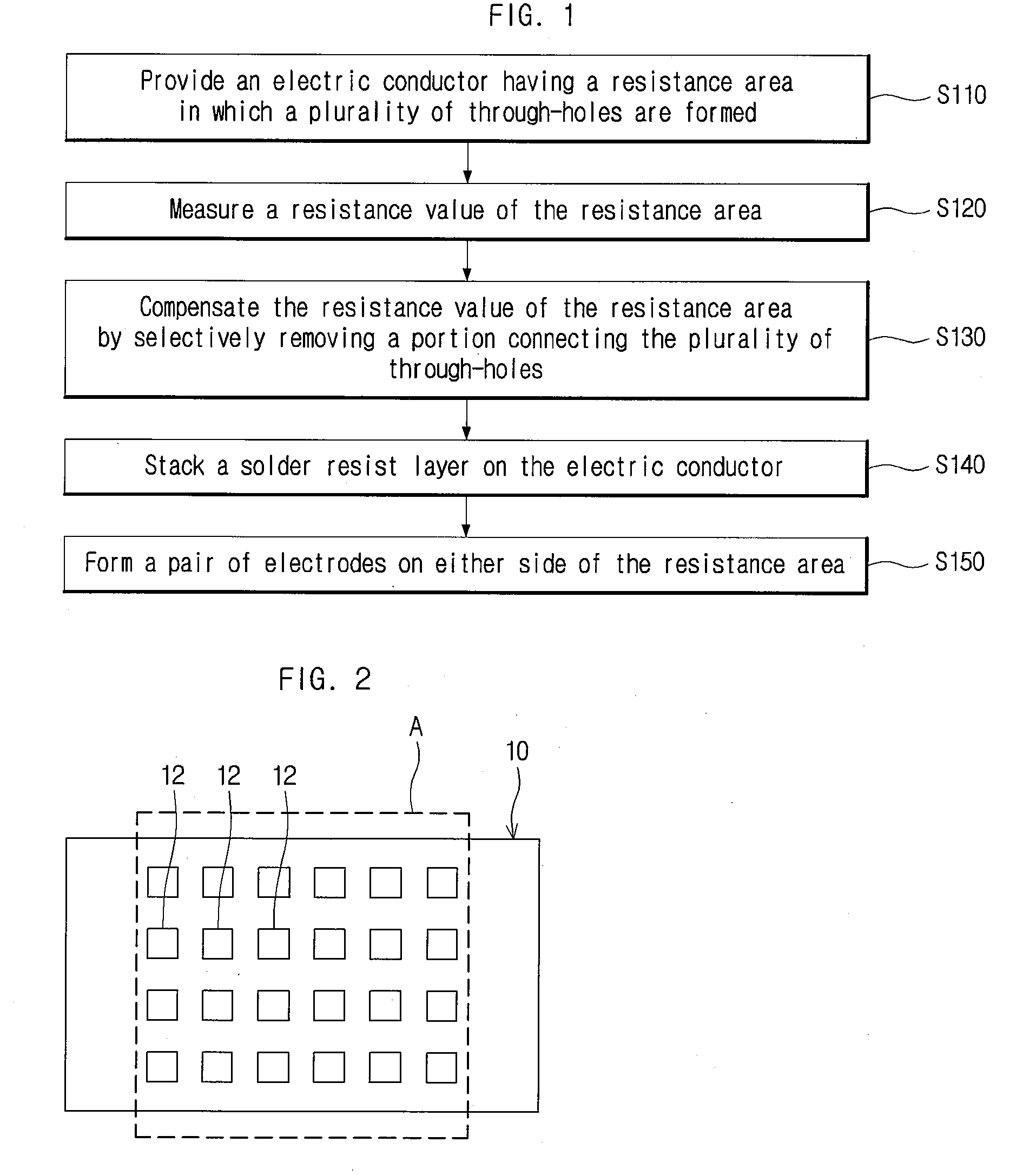
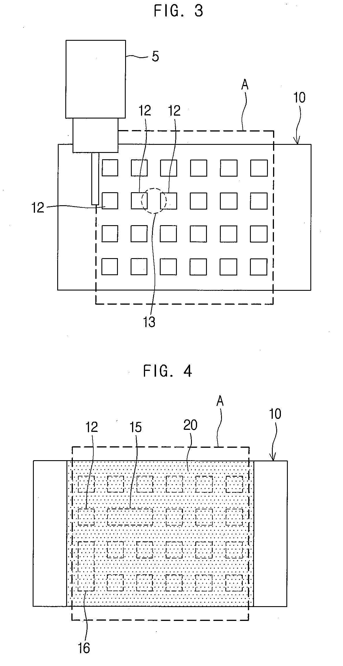
[0020]FIG. 1 is a flow diagram illustrating a method of forming a resistor in accordance with an embodiment of the present invention, and FIG. 2 to FIG. 6 illustrate a method of forming a resistor in accordance with an embodiment of the present invention.
[0021]The method of forming a resistor in accordance with an embodiment of the present invention includes providing an electric conductor (S110), measuring a resistance value (S12) and compensating the resistance value (S130).
[0022]In the step of providing an electric conductor (S110), an electric conductor 10, in which a plurality of through-holes 12 are formed, is provided. The area in which the plurality of through-holes 12 are formed becomes a resistance area A that forms electric resistance.
[0023]The electric conductor 10 is a material, such as metal, which has a high conductivity of electricity, that is, a...
PUM
| Property | Measurement | Unit |
|---|---|---|
| Electrical resistance | aaaaa | aaaaa |
Abstract
Description
Claims
Application Information


