Process for producing a base connection of a bipolar transistor

a bipolar transistor and base connection technology, applied in the direction of transistors, electrical devices, semiconductor devices, etc., can solve the problems of reducing the electrical properties of the resulting component, affecting the electrical properties of the component, and requiring the process from d2 for selective epitaxy, so as to achieve low resistance and capacitance values, and simplify manufacturing

Inactive Publication Date: 2005-10-06
ATMEL CORP
View PDF20 Cites 5 Cited by
  • Summary
  • Abstract
  • Description
  • Claims
  • Application Information

AI Technical Summary

Benefits of technology

[0033] In a process according to an embodiment of the invention, the semiconductor structure can be covered with the first semiconductor layer and the reaction layer without additional masking steps (i.e., non-selectively), thereby simplifying manufacture. The three-dimensional sacrificial structure, which to some extent can serve as a mask, does not represent an additional mask in this regard, since it can be used multiple times in conjunction with later process steps. Thus, it later defines the extent of a hollow form for a lithography-independent, self-aligning creation of an emitter layer. The use of the three-dimensional structure to cover the inner base during creation of the semiconductor layer that can be later silicidized results in silicide traces that come very close to the inner base, which is advantageous for a low-resistance connection to the inner base. A perfect isolation of the base connection in the vertical direction is achieved by the partial exposure of the first semiconductor layer, the removal of the reaction products in the exposed areas, and the filling of the semiconductor structure above the silicidized layer. Overall, the result is a base connection with a sharply reduced barrier-layer transistor having low resistance and capacitance values.
[0034] In the course of further processing of the structure created by the process into a bipolar transistor, the regions made up of the low-resistivity compound can become part of the structures which electrically contact the base of the bipolar transistor. An opening extending between inside spacers will define the position of the emitter window relative to the regions of the low-resistivity compound in a self-aligning manner. The second dielectric layer and the inside spacers can therefore electrically insulate the regions of the low-resistivity compound from the structures that electrically contact the emitter region.

Problems solved by technology

However, compounds of the metal and germanium exhibit poor thermal stability and dissociate at the silicide transition temperature.
While the junction transistor can utilize the advantages resulting from the alloying of germanium with the silicon material of the inner base, this is not the case for the surface-barrier transistor, so the large-area surface-barrier transistor adversely affects the electrical properties of the resulting component.
However, the requirement in the process from D2 for selective epitaxy, a complex and expensive epitaxy process, is a disadvantage.

Method used


Image

  • Process for producing a base connection of a bipolar transistor
  • Process for producing a base connection of a bipolar transistor
  • Process for producing a base connection of a bipolar transistor

Examples


Embodiment Construction

[0067] In the drawings, like elements are labeled with like reference symbols.

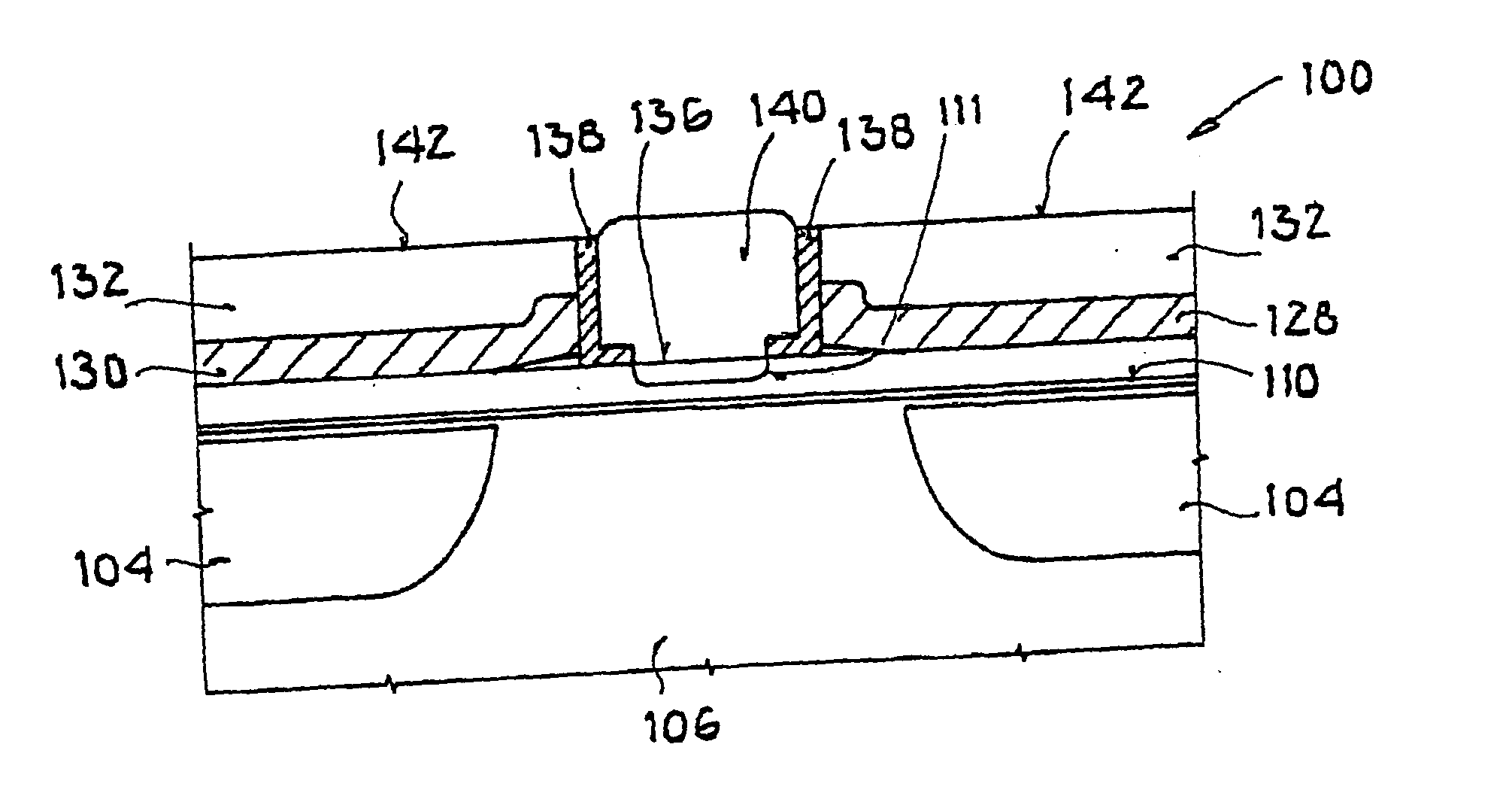
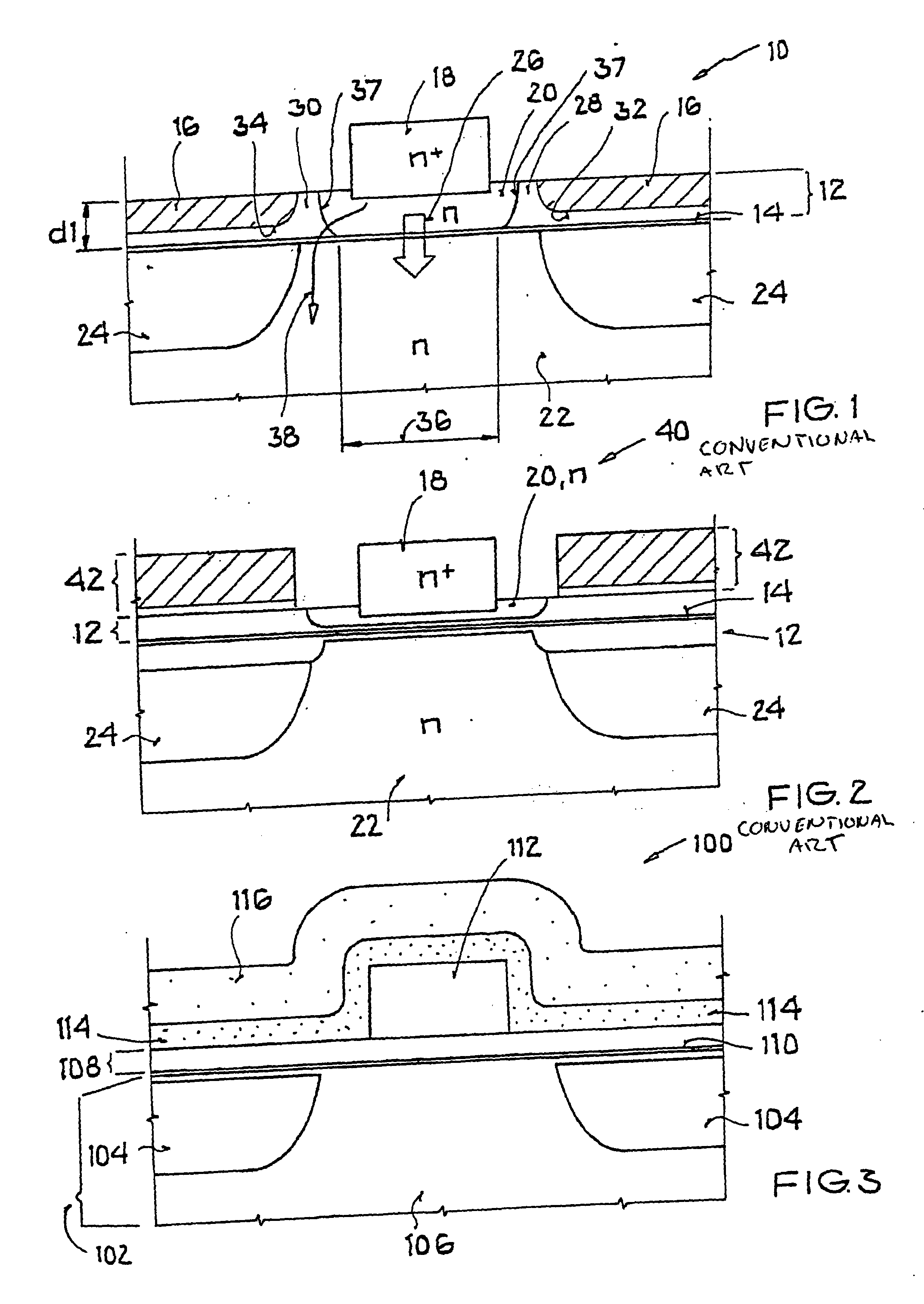
[0068] In FIG. 1, which illustrates a first conventional process as described above, number 10 designates a semiconductor structure with a comparatively thick doped silicon layer 12, e.g., the layer of thickness d1 over a thin SiGe base layer 14. The thickness d1 is dimensioned here such that sufficient material is available for silicidizing the base connection. Hatched regions 16 represent silicidized regions. Block 18 represents a highly n-doped emitter region. The number 20 designates a less highly n-doped emitter region, and the number 22 designates an n-doped collector region with a lateral STI isolation 24. The section of the semiconductor structure 10 shown thus contains a hetero-bipolar transistor (HBT) having emitter regions 18, 20, SiGe base layer 14, and collector region 22. The number 26 represents a regular HBT current flowing in later operation. In such an HBT implementation having a thick s...


PUM


Abstract

A process for producing a base connection of a bipolar transistor is provided. The process includes the steps of providing a semiconductor structure that can include a three-dimensional sacrificial structure that is selectively removable with respect to adjacent regions. A first semiconductor layer and a second layer of dielectric material is deposited. The first semiconductor layer is partially exposed by partial removal of the second layer. A first reaction layer is deposited that, together with the first semiconductor layer forms reaction products, which are selectively removable with respect to adjacent regions. Remaining material of the first reaction layer that has not reacted with the material of the first semiconductor layer is removed. A second reaction layer is deposited that, with the first semiconductor layer, forms a low-resistivity compound. Remaining material of the second reaction layer that has not reacted with the material of the first semiconductor layer is removed. An additional dielectric layer is deposited and the sacrificial structure is exposed by partial removal of the additional dielectric layer. Dielectric inner spacers are provided in an aperture formed by removal of the sacrificial structure.

Description

[0001] This nonprovisional application claims priority under 35 U.S.C. § 119(a) on German Patent Application No. DE 102004017166.1, which was filed in Germany on Apr. 1, 2004, and which is herein incorporated by reference. BACKGROUND OF THE INVENTION [0002] 1. Field of the Invention [0003] The present invention relates to a process for producing a base connection of a bipolar transistor having active regions of a first conductivity type, active regions of a second conductivity type, and low-resistivity regions of semiconductor / metal mixed crystals that connect to an inner subregion of the active regions of the second conductivity type in an electrically conductive manner. [0004] 2. Description of the Background Art [0005] A base of a bipolar transistor manufactured with a planar process can be conceptually divided into an inner base and an outer base. The inner base forms flat, parallel pn junctions with adjacent emitter and collector layers, while the outer base provides electrical...

Claims


Application Information

Patent Timeline
Patent Type & Authority Applications(United States)
IPC IPC(8): H01L21/8222H01L21/331H01L29/10H01L29/423
CPCH01L29/1004H01L29/42304H01L29/66242
Inventor BROMBERGER, CHRISTOPH
Owner ATMEL CORP
Why Eureka
Try Eureka