
Display unit, method of manufacturing display unit, and electronic apparatus

Active Publication Date: 2017-10-05
SONY CORP
View PDF15 Cites 10 Cited by
  • Summary
  • Abstract
  • Description
  • Claims
  • Application Information

AI Technical Summary

Benefits of technology

The present patent provides a display unit, method of manufacturing the display unit, and electronic apparatus that can improve luminance while reducing power consumption. This is done by improving the efficiency of extracting light emitted from the organic layer through a reflector layer with a light-reflecting surface. Additionally, an auxiliary electrode is provided on the reflector layer that is exposed from the organic layer and is covered with the second electrode to secure electrical connection. This helps in reducing a resistance value in the second electrode without increasing its film thickness and becomes possible by securing the low-resistance connection between the auxiliary electrode and the second electrode.

Problems solved by technology

As a result, a voltage is dropped (occurrence of so-called voltage drop) at a middle portion of a panel, causing an increase in power consumption as well as deterioration of image quality.
In this case, use of metal for the upper electrode enables the resistance to be lowered; however, metal has poor light-transmissivity.
Thus, the use of metal for the upper electrode reduces light extraction efficiency, causing luminance to be lowered.
When the transparent electrically conductive film has increased thickness, however, the light-transmissivity is lowered, leading to lowered luminance.
As described, it is not easy for the upper electrode to both achieve light-transmissivity and electrical conductivity.

Method used


Image

  • Display unit, method of manufacturing display unit, and electronic apparatus
  • Display unit, method of manufacturing display unit, and electronic apparatus
  • Display unit, method of manufacturing display unit, and electronic apparatus

Examples


embodiment

Configuration

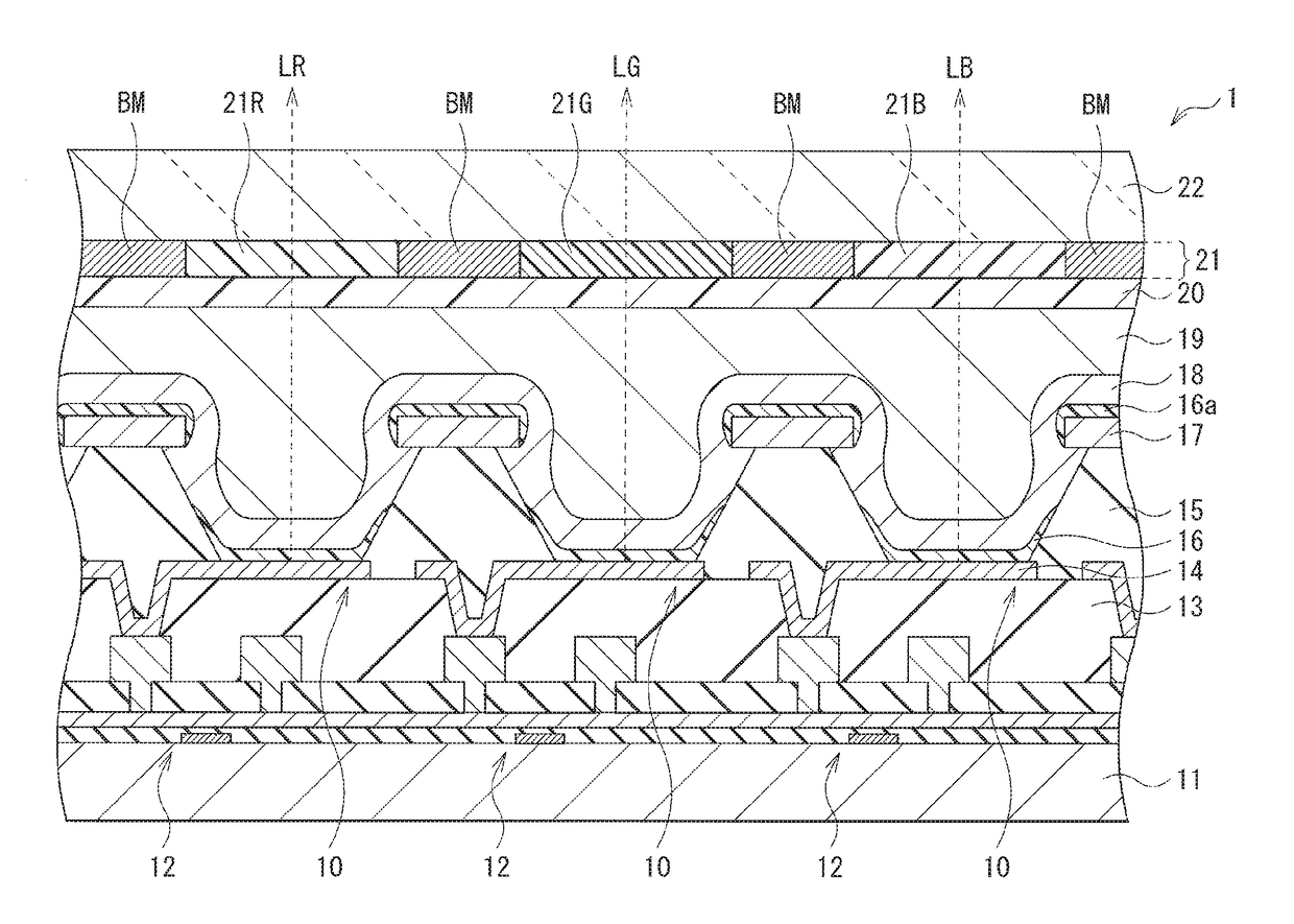
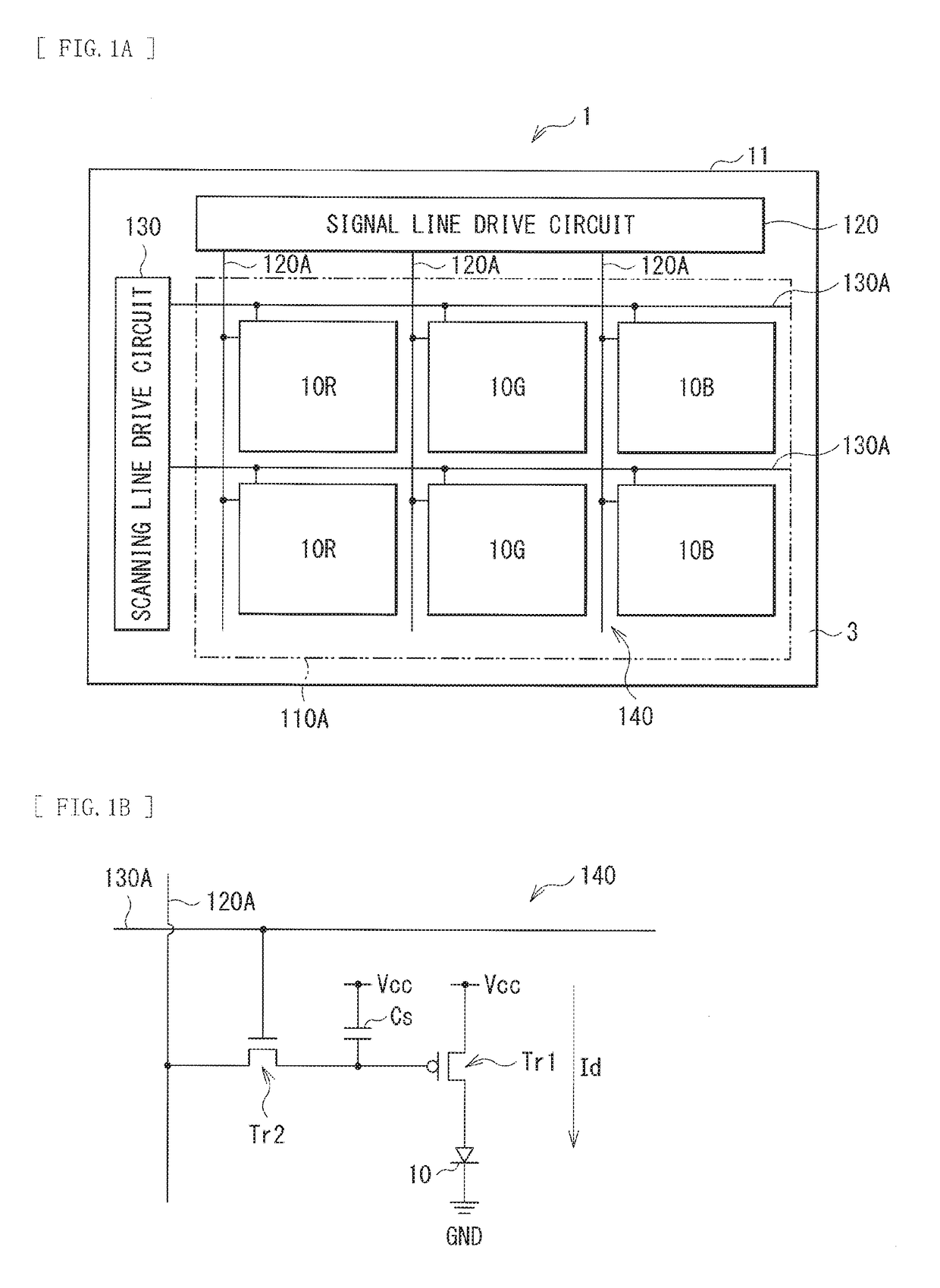
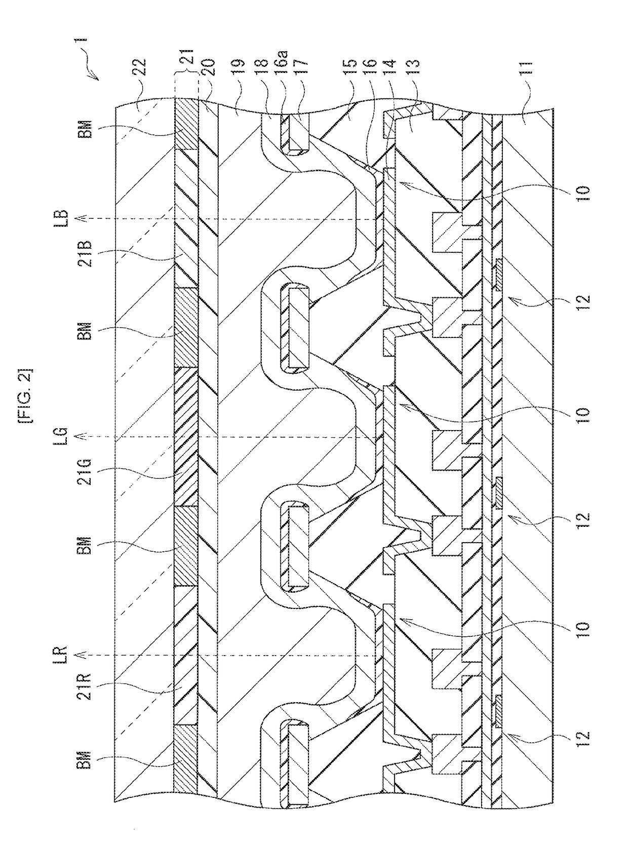
[0049]FIG. 1A illustrates a configuration of a display unit (display unit 1) according to an embodiment of the present disclosure. The display unit 1 may be an organic EL display. In a display region 110A on a first substrate 11, a plurality of pixels 10R, 10G, and 10B each including an organic EL device 10 may be disposed in matrix. The pixels 10R, 10G, and 10B emit, respectively, red light LR (wavelength of 620 nm to 750 nm both inclusive), green light LG (wavelength of 495 nm to 570 nm both inclusive), and blue light LB (wavelength of 450 nm to 495 nm both inclusive). The pixels 10R, 10G, and 10B may correspond to subpixels (R pixel, G pixel, and B pixel); for example, a combination of the R pixel, the G pixel, and the B pixel may be adopted as one pixel to perform image display. On the periphery of the display region 110A, there may be provided a signal line drive circuit 120 and a scanning line drive circuit 130 for image display.

[0050]An active drive circuit (pixe...

application examples

[0085]The display unit described in the foregoing embodiment and modification example is applicable to electronic apparatuses in any fields that display, as an image, an image signal input from outside or an image signal generated inside. The display unit described herein is particularly suitable for small-sized to mid-sized electronic apparatuses. The followings illustrate examples thereof.

[0086]FIGS. 7A and 7B illustrate outer appearances of a smartphone 220. The smartphone 220 may include, for example, a display section 221 and an operation section 222 on front side, and a camera 223 on rear side; the display unit 1 of the foregoing embodiment may be mounted on the display section 221.

[0087]FIG. 8 illustrates an outer appearance of a tablet personal computer 240. The tablet personal computer 240 may include, for example, a touch panel section 241 and a casing 242; the display unit 1 of the foregoing embodiment may be mounted on the touch panel section 241.

[0088]FIG. 9 illustrates...


PUM


Abstract

A display unit includes a plurality of pixels, a reflector layer, and an auxiliary electrode. Each of the plurality of pixels has a first electrode, an organic layer, and a second electrode in this order. The organic layer and the second electrode are provided on the first electrode. The organic layer includes a light-emitting layer. The reflector layer has a light-reflecting surface around each of the pixels. The auxiliary electrode is provided on the reflector layer and is projected from an upper end of the light-reflecting surface. The auxiliary electrode has a portion which is exposed from the organic layer, and the exposed portion is covered with the second electrode.

Description

TECHNICAL FIELD[0001]The present disclosure relates to a display unit such as an organic electroluminescence unit, a method of manufacturing the display unit, and an electronic apparatus including the display unit.BACKGROUND ART[0002]Recently, display units with use of an organic electroluminescence (EL) device (organic EL displays) have been increasingly developed. The display units are roughly classified into top surface emission (top emission) display units and bottom surface emission (bottom emission) display units.[0003]In the top surface emission display unit, an upper electrode (e.g., cathode) on light extraction side is typically configured by a transparent electrically conductive film such as indium-tin oxide (ITO), thus causing resistance (cathode resistance) to be high. As a result, a voltage is dropped (occurrence of so-called voltage drop) at a middle portion of a panel, causing an increase in power consumption as well as deterioration of image quality. In this case, us...

Claims


Application Information

Patent Timeline
IPC IPC(8): H01L51/52H01L27/32H01L51/56
CPCH01L51/5271H01L27/322H01L51/5228H01L51/56H10K59/38H10K59/122H10K50/824H10K50/856H10K71/00
Inventor UEDA, DAISUKE
Owner SONY CORP
Learn More