
Light emitting diode chip having wavelength converting layer and method of fabricating the same, and package having the light emitting diode chip and method of fabricating the same

Active Publication Date: 2011-11-24
SEOUL SEMICONDUCTOR
View PDF9 Cites 99 Cited by
  • Summary
  • Abstract
  • Description
  • Claims
  • Application Information

AI Technical Summary

Benefits of technology

[0014]Exemplary embodiments of the present invention provide an LED chip capable of preventing light converted in a wavelength converting layer from being incident into the LED chip.
[0015]Exemplary embodiments of the present invention provide an LED chip capable of preventing a wavelength converting layer from being damaged by light.

Problems solved by technology

However, as the resin is applied in the package, the phosphor may not be uniformly distributed in the resin, and it may be difficult to form the resin having a uniform thickness.
However, since the wavelength converting sheet is attached on the top surface of the LED, it may be limited to implement white light in an LED in which light is configured to be mostly emitted through the top surface of the LED.
Further, the wavelength conversion using the wavelength converting sheet may not be suitable in an LED in which a considerable amount of light is configured to be emitted through side surfaces of the LED, e.g., to side surfaces of a growth substrate.

Method used


Image

  • Light emitting diode chip having wavelength converting layer and method of fabricating the same, and package having the light emitting diode chip and method of fabricating the same
  • Light emitting diode chip having wavelength converting layer and method of fabricating the same, and package having the light emitting diode chip and method of fabricating the same
  • Light emitting diode chip having wavelength converting layer and method of fabricating the same, and package having the light emitting diode chip and method of fabricating the same

Examples


Embodiment Construction

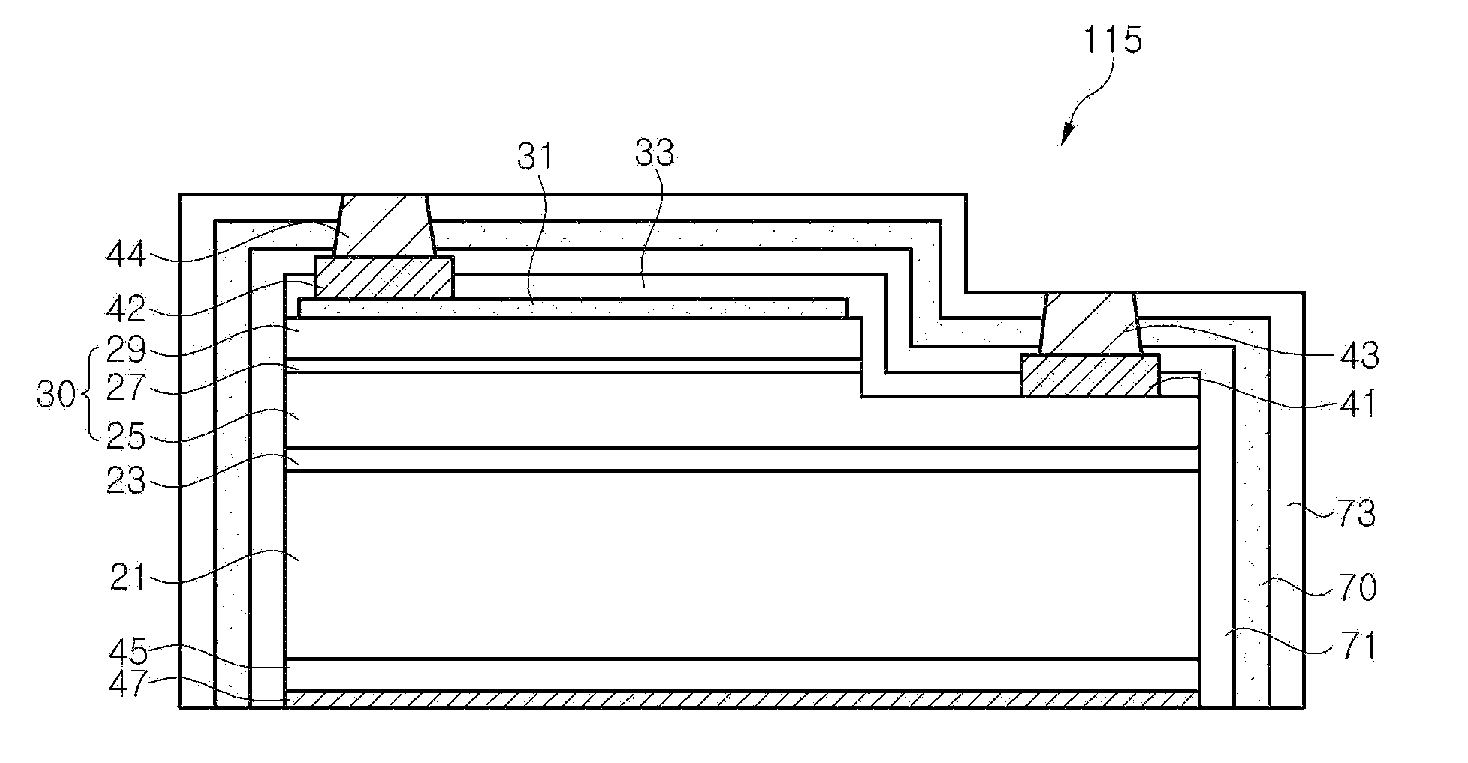
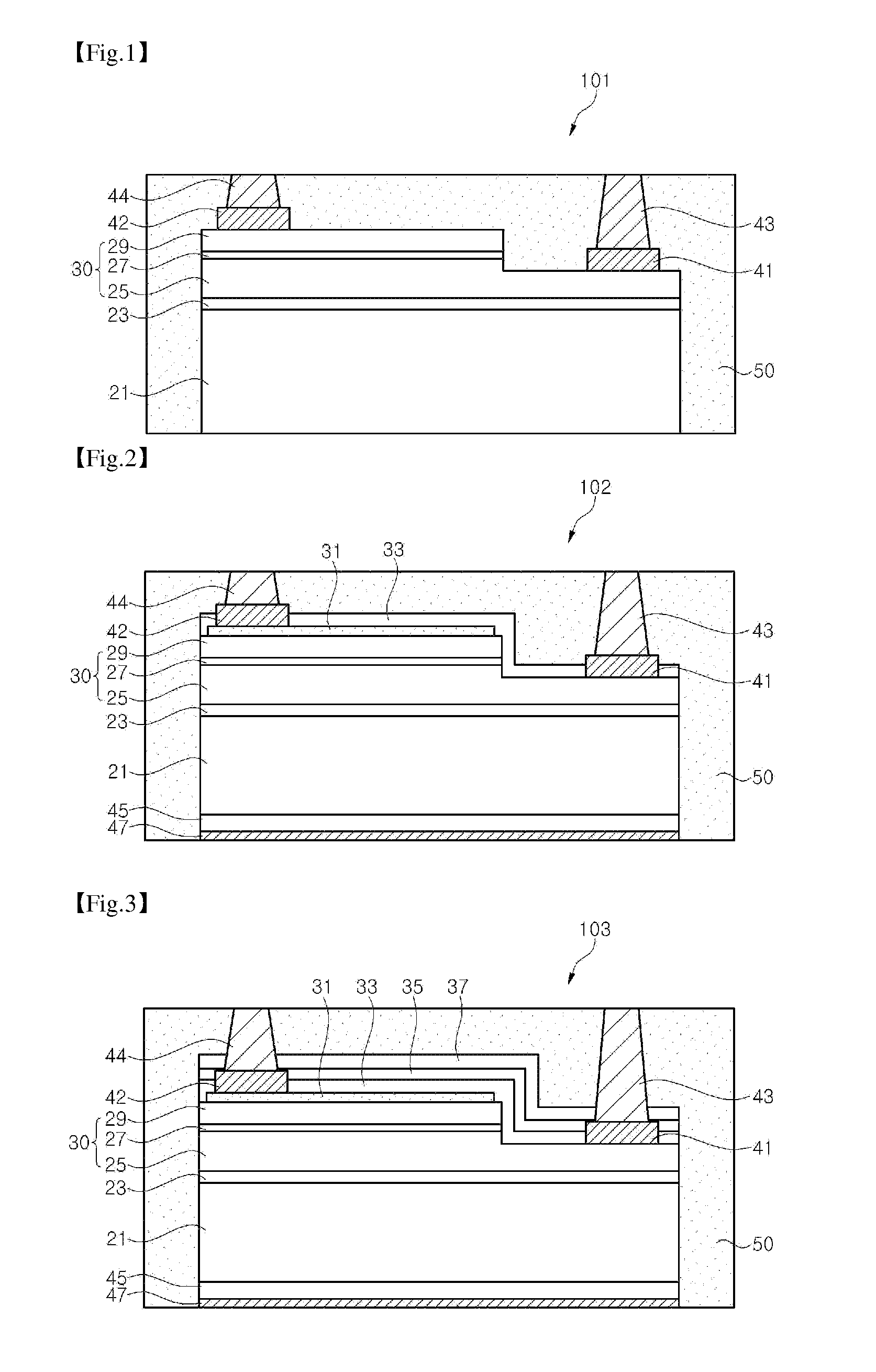
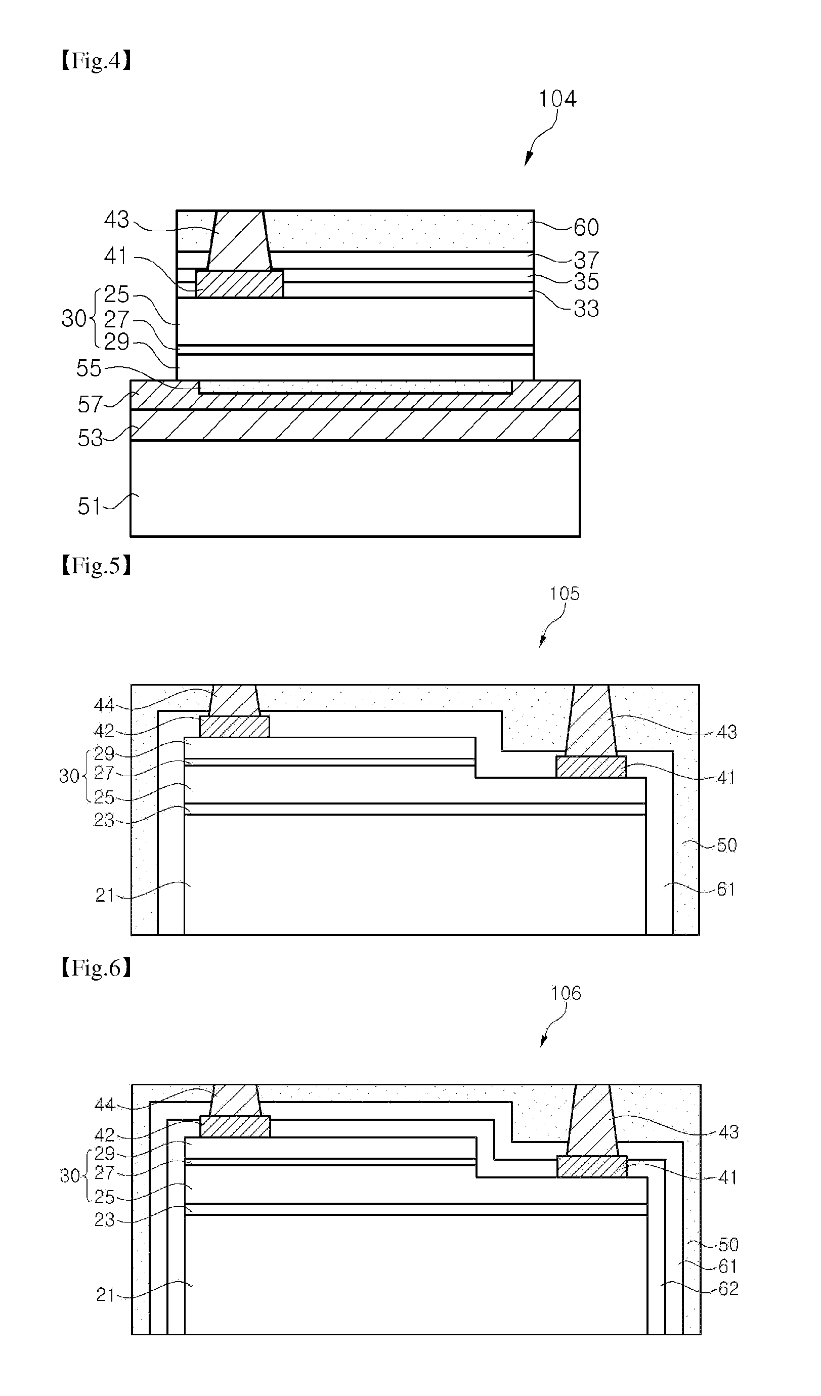
[0053]Hereinafter, exemplary embodiments of the present invention will be described in detail with reference to the accompanying drawings. The following exemplary embodiments are provided only for illustrative purposes so that those skilled in the art can fully understand the spirit of the present invention. Therefore, the present invention is not limited to the following exemplary embodiments but may be implemented in other forms. In the drawings, the widths, lengths, thicknesses and the like of elements may be exaggerated for convenience of illustration. Like reference numerals indicate like elements throughout the specification and drawings.

[0054]It will be understood that when an element or layer is referred to as being “on” or “connected to” another element or layer, it can be directly on or directly connected to the other element or layer, or intervening elements or layers may be present. In contrast, when an element is referred to as being “directly on” or “directly connected...


PUM


Abstract

An exemplary embodiment of the present invention discloses an LED chip including a substrate, a GaN-based compound semiconductor stacked structure arranged on the substrate, an electrode electrically connected to the semiconductor stacked structure, and a wavelength converting layer covering a portion of the semiconductor stacked structure. The electrode passes through the wavelength converting layer. The semiconductor stacked structure includes a first conductivity-type semiconductor layer, an active layer, and a second conductivity-type semiconductor layer.

Description

CROSS-REFERENCE TO RELATED APPLICATIONS[0001]This application claims priority from and the benefit of Korean Patent Application No. 10-2010-0046423, filed on May 18, 2010, Korean Patent Application No. 10-2010-0090352, filed on Sep. 15, 2010, Korean Patent Application No. 10-2010-0096682, filed on Oct. 5, 2010 and Korean Patent Application No. 10-2010-0110149, filed on Nov. 8, 2010, which are hereby incorporated by reference for all purposes as if fully set forth herein.BACKGROUND OF THE INVENTION[0002]1. Field of the Invention[0003]The present invention relates to a light emitting diode (LED) chip and a method of fabricating the same, and a package having the LED chip and a method of fabricating the same, and more particularly, to an LED chip having a wavelength converting layer and a method of fabricating the same, and a package having the LED chip and a method of fabricating the same.[0004]2. Discussion of the Background[0005]LEDs are currently used as backlight sources in variou...

Claims


Application Information

Patent Timeline
IPC IPC(8): H01L33/06H01L33/46H01L33/62H01L33/38H01L33/12H01L33/50H01L33/32
CPCH01L25/0753H01L33/44H01L33/505H01L2224/48091H01L2224/48227H01L33/50H01L33/06H01L2924/00014H01L2924/00H01L33/46H01L33/56
Inventor JUNG, JUNG HWAKIM, BANG HYUN
Owner SEOUL SEMICONDUCTOR
Features
  • Generate Ideas
  • Intellectual Property
  • Life Sciences
  • Materials
  • Tech Scout
  • Unparalleled Data Quality
  • Higher Quality Content
  • 60% Fewer Hallucinations
Learn More