

Circuit board with conductor post structure
a conductor and circuit board technology, applied in the direction of semiconductor/solid-state device details, soldering apparatus, manufacturing tools, etc., can solve the problems of increasing the footprint of the pre-solder, reducing and limiting the bump pitch to minimum, so as to reduce the thickness of the solder mask
- Summary
- Abstract
- Description
- Claims
- Application Information
AI Technical Summary
Benefits of technology
Problems solved by technology
Method used
Image

Examples
Embodiment Construction
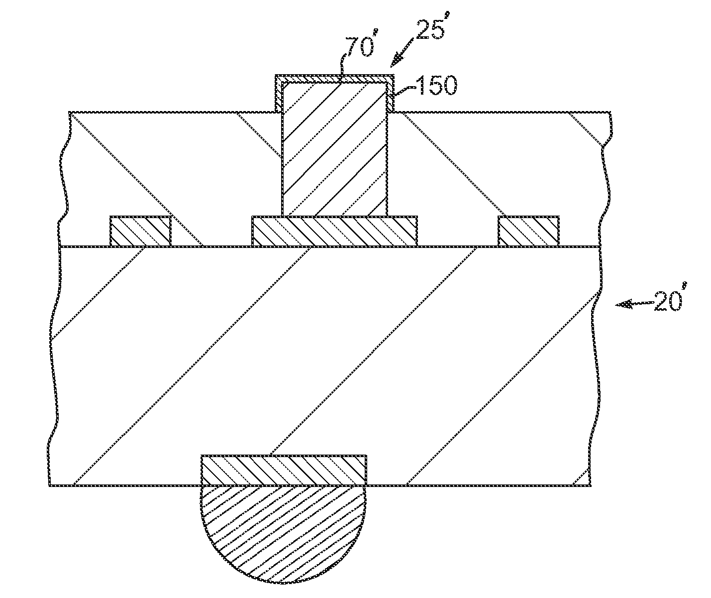
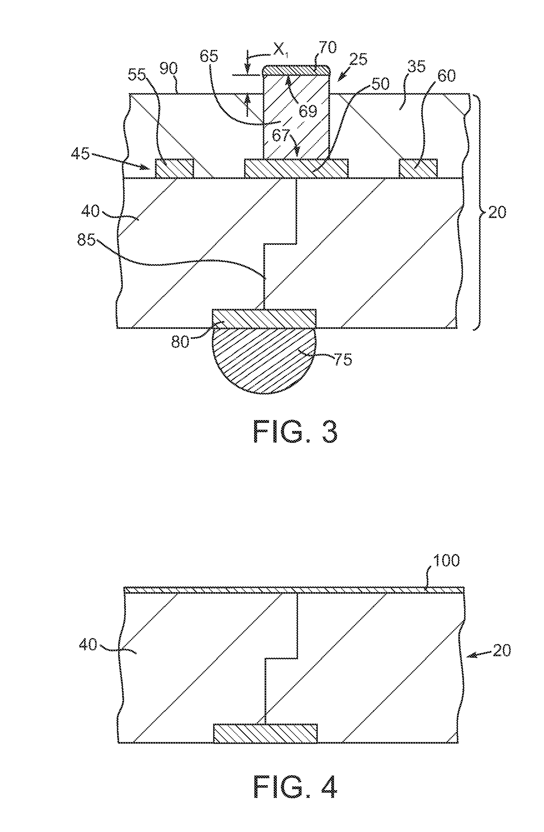
[0009]In accordance with one aspect of an embodiment of the present invention, a method of manufacturing is provided that includes forming a conductor post on a side of a circuit board. The conductor post includes an end projecting away from the side of the circuit board. A solder mask is applied to the side of the circuit board to cover the conductor post. A thickness of the solder mask is reduced so that a portion of the conductor post projects beyond the solder mask.
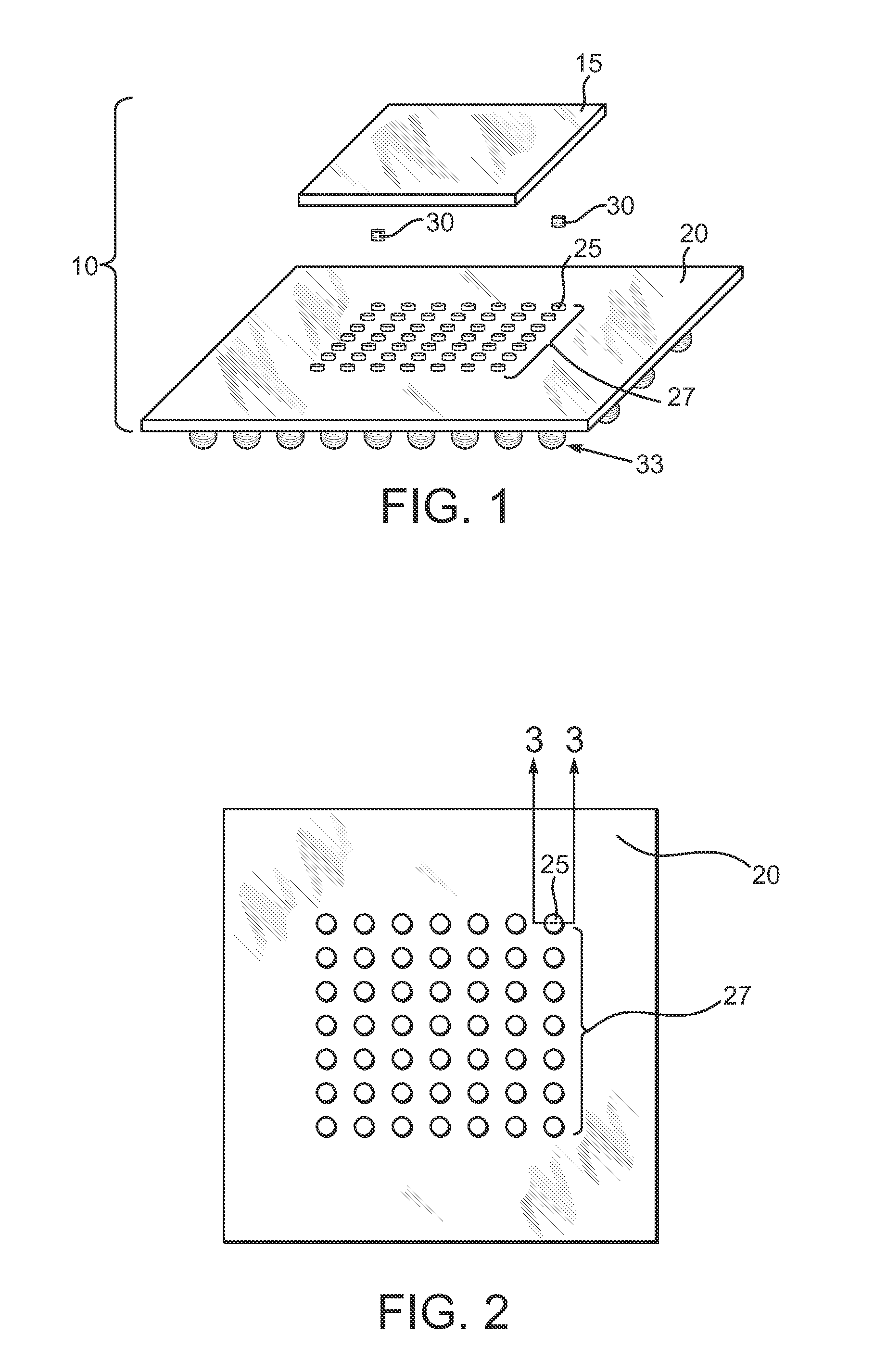
[0010]In accordance with another aspect of an embodiment of the present invention, a method of manufacturing is provided that includes forming plural conductor posts on a side of a semiconductor chip package substrate. Each of the conductor posts includes an end projecting away from the side of the circuit board. A solder mask is applied to the side of the semiconductor chip package substrate to cover the plural conductor posts. A thickness of the solder mask is reduced so that a portion of each of the conductor posts...
PUM
| Property | Measurement | Unit |
|---|---|---|
| Thickness | aaaaa | aaaaa |
| Electrical conductor | aaaaa | aaaaa |
Abstract
Description
Claims
Application Information