Camera Module with Premolded Lens Housing and Method of Manufacture

a technology of camera modules and lens housings, applied in the field of digital cameras, can solve the problems of image capture devices that are extremely sensitive, disadvantages in terms of manufacturing time, cost, quality and yield of camera modules, and image capture devices that are extremely vulnerable to damage and contamination

Inactive Publication Date: 2011-12-08
SHANGGUAN DONGKAI +1
View PDF20 Cites 4 Cited by
  • Summary
  • Abstract
  • Description
  • Claims
  • Application Information

AI Technical Summary

Benefits of technology

[0009]The present invention overcomes the problems associated with the prior art by providing a digital camera module and a method of manufacturing the camera module, wherein the housing is mounted to the circuit substrate before the image capture device is mounted to the circuit substrate. Mounting the housing onto the circuit substrate before mounting the image capture device onto the circuit substrate prevents the image capture device from being damaged during the housing attachment process. In addition, having the housing attached to the circuit substrate provides a more robust substrate to mount the image capture device on.
[0011]In one embodiment, the structure of the housing facilitates the later mounting of the image capture device. The housing includes a bore with a diameter that is larger than a diagonal of the image capture device, so the image capture device can be mounted through the bore. In another embodiment, the position of the housing facilitates the later mounting of the image capture device. The housing is fixed to one surface (e.g., the top) of the circuit substrate and the image capture device is mounted to the opposite surface (e.g., the bottom) of the circuit substrate. In this embodiment, the circuit substrate defines an aperture and the image capture device is mounted so that light passing through the aperture impinges on a light sensitive portion of the image capture device.

Problems solved by technology

The image capture devices are very sensitive, which is a disadvantage in terms of manufacturing time, cost, quality, and yield of the camera module.
The image capture device is extremely vulnerable to damage and contamination, particularly before and during the housing attach process.
For example, before the housing is attached to the circuit substrate, the wire bonds are exposed to inadvertent contact (e.g., during handling), which can cause damage.
Further, the image capture device is vulnerable to contamination from particulate debris caused by the housing attach process.
Contamination of the sensor array will block light and cause visible artifacts in every image captured by the device.
Obviously, damaged image capture devices causes a decrease in product yield and an increase in labor and material costs.

Method used


Image

  • Camera Module with Premolded Lens Housing and Method of Manufacture
  • Camera Module with Premolded Lens Housing and Method of Manufacture
  • Camera Module with Premolded Lens Housing and Method of Manufacture

Examples


Embodiment Construction

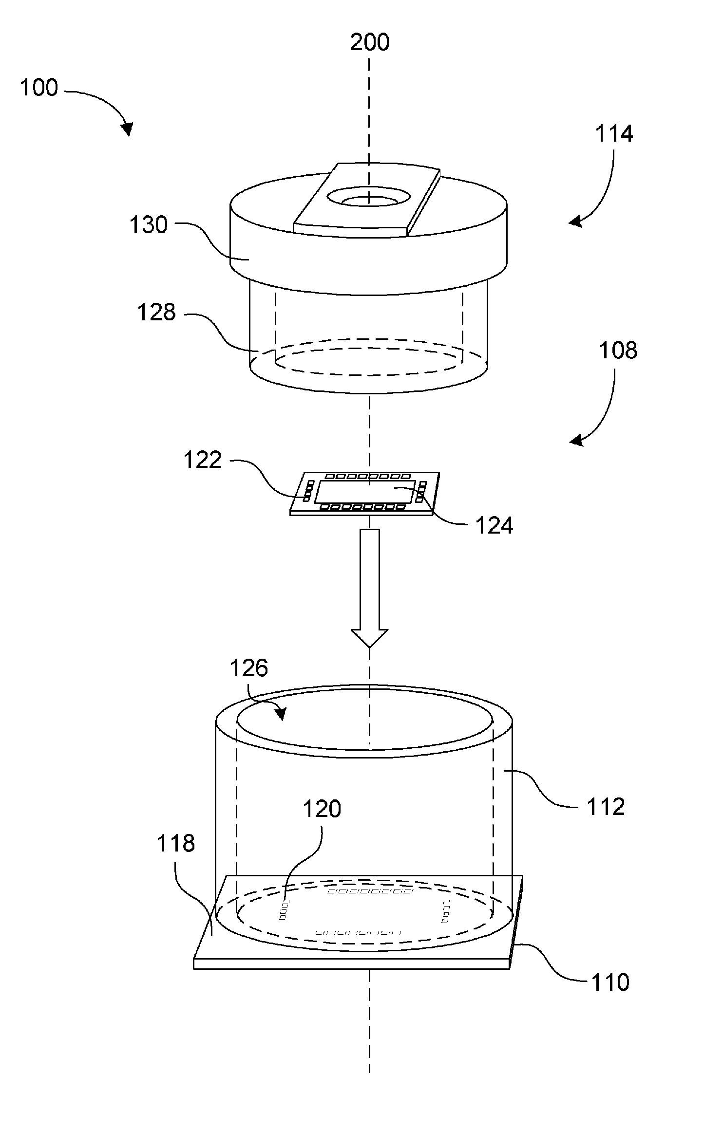
[0024]The present invention overcomes the problems associated with the prior art, by providing a system and method for manufacturing a digital camera module, wherein a housing adapted to hold a lens unit is mounted on a substrate prior to mounting an image capture device on the substrate. In the following description, numerous specific details are set forth (e.g., example lens housing structure, etc.) in order to provide a thorough understanding of the invention. Those skilled in the art will recognize, however, that the invention may be practiced apart from these specific details. In other instances, details of well known camera module manufacturing practices (e.g., assembly, circuit fabrication, molding processes, focusing means, etc.) and components have been omitted, so as not to unnecessarily obscure the present invention.

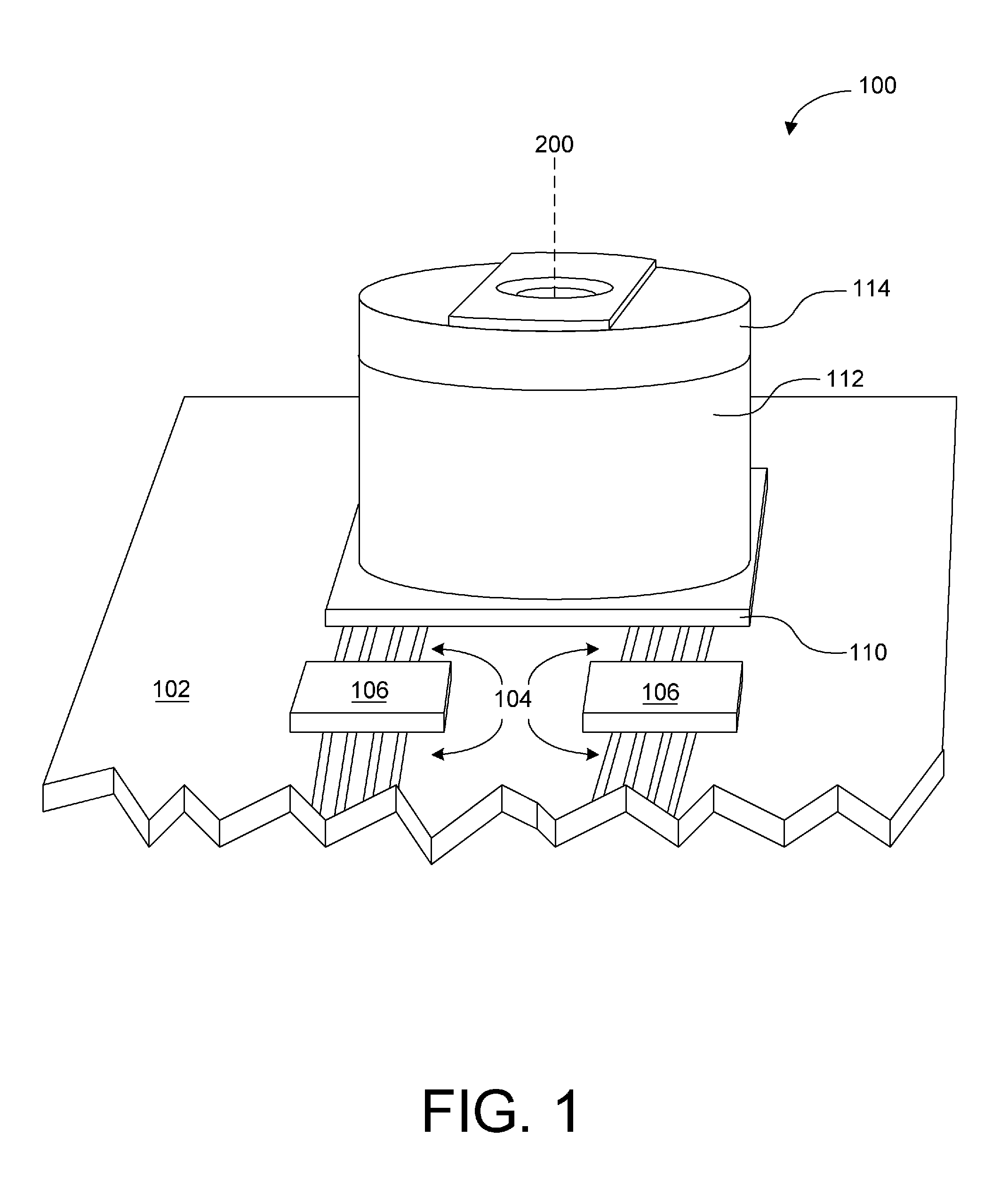
[0025]FIG. 1 is a perspective view of a camera module 100 according to one embodiment of the present invention. Camera module 100 is shown mounted on a circui...


PUM

PropertyMeasurementUnit
insulatingaaaaaaaaaa
conductiveaaaaaaaaaa
electricalaaaaaaaaaa

Abstract

A novel digital camera module includes an image capture device, a circuit substrate, a lens unit and a housing that is mounted to the circuit substrate before the image capture device is mounted to the circuit substrate. In one particular embodiment, the housing is formed onto the circuit substrate via molding. The housing includes a bore to receive the lens unit, with the diameter of the bore being larger than the diagonal of the image capture device such that image capture device can be mounted to the circuit substrate through the bore. In another particular embodiment, the circuit substrate includes an aperture so as to facilitate the flip-chip bonding of the image capture device. The order in which the image capture device and the housing are coupled to the circuit substrate helps prevent damage to the image capture device during the mounting of the housing to the circuit substrate.

Description

RELATED APPLICATIONS[0001]This application is a continuation of co-pending U.S. patent application Ser. No. 11 / 444,277, filed May 31, 2006 by the same inventors, which is incorporated herein by reference in its entirety.BACKGROUND OF THE INVENTION[0002]1. Field of the Invention[0003]The present invention relates generally to digital cameras, and more particularly to digital camera modules that can be mounted in host electronic devices. Even more particularly, the present invention relates to a process for manufacturing a digital camera module that substantially reduces potential damage to an image capture device during the manufacturing the digital camera or digital camera module.[0004]2. Description of the Background Art[0005]Digital camera modules are currently being incorporated into a variety of electronic devices. Such camera hosting devices include, but are not limited to, cellular telephones, personal digital assistants (PDAs), and computer cams. The demand for digital camera...

Claims


Application Information

Patent Timeline
Patent Type & Authority Applications(United States)
IPC IPC(8): G03B17/00H05K13/00G03B17/02H04N5/225
CPCG03B17/02H04N5/2257H01L2224/49175Y10T29/49002H01L2224/48091H01L2224/48464H01L2924/00014H01L2224/05554H04N23/57
Inventor SHANGGUAN, DONGKAITAM, SAMUEL WAISING
Owner SHANGGUAN DONGKAI
Why Eureka
Try Eureka