
Method for manufacturing semiconductor chips from a semiconductor wafer

Active Publication Date: 2011-12-08
STMICROELECTRONICS (TOURS) SAS
View PDF2 Cites 7 Cited by
  • Summary
  • Abstract
  • Description
  • Claims
  • Application Information

AI Technical Summary

Benefits of technology

[0015]Thus, an embodiment provides a method for manufacturing semiconductor chips from a semiconductor wafer, which overcomes at least some of the disadvantages of existing methods.
[0017]An embodiment provides such a method which is easy to implement.

Problems solved by technology

Accordingly, in such a production system, a manufacturer of semiconductor chips using a given type of frame can only sell his production to users equipped to receive this type of frame.

Method used


Image

  • Method for manufacturing semiconductor chips from a semiconductor wafer
  • Method for manufacturing semiconductor chips from a semiconductor wafer
  • Method for manufacturing semiconductor chips from a semiconductor wafer

Examples


Embodiment Construction

[0033]For clarity, the same elements have been designated with the same reference numerals in the different drawings and, further, the various drawings are not to scale.

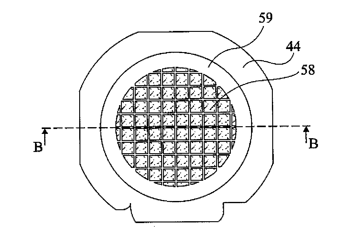
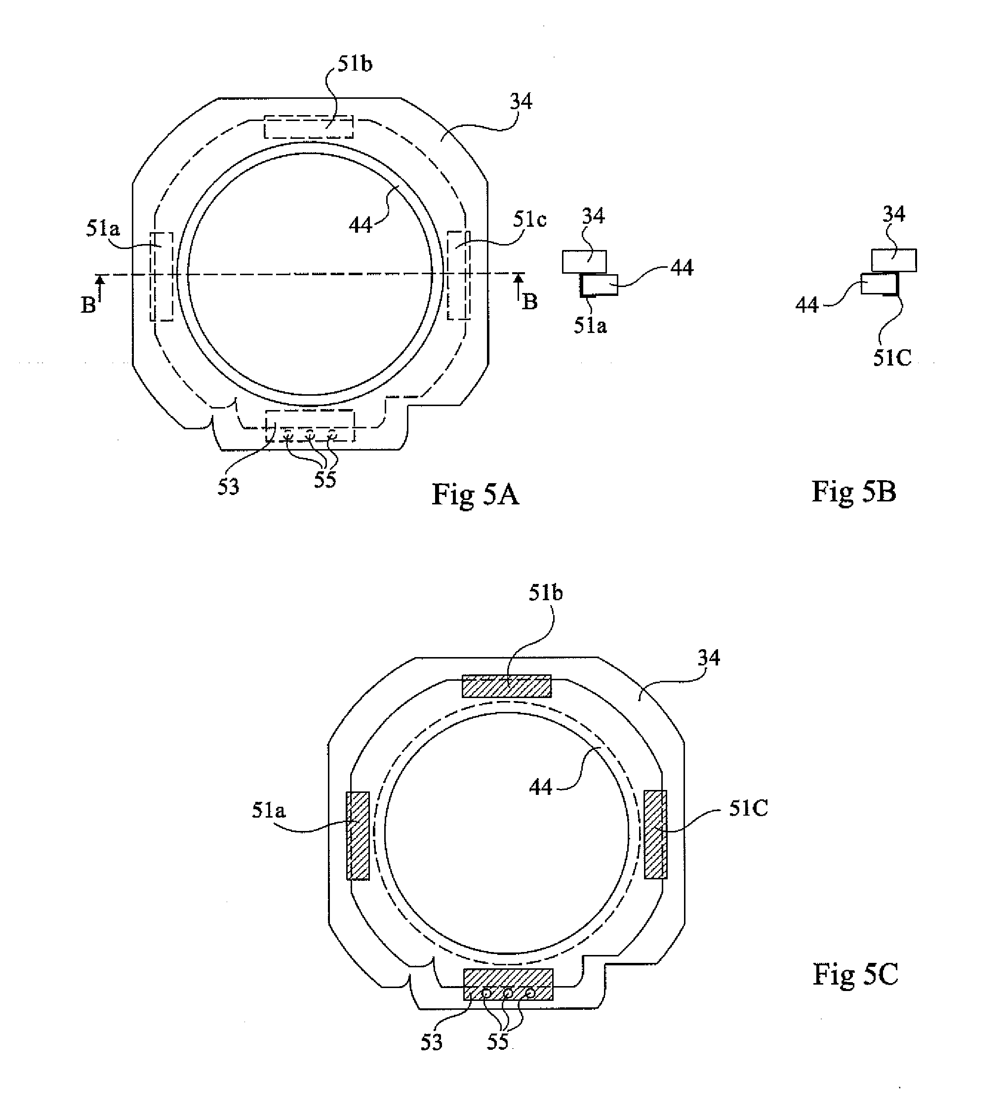
[0034]FIGS. 5A, 5B, 5C, 6A, 6B, 7A, 7B, and 8A, 8B schematically illustrate steps of a method for manufacturing semiconductor chips, capable of producing, in a production line specifically adapted to process semiconductor wafers arranged on a frame 34 of the type described in relation with FIG. 3, chips arranged on a frame 44 of the type described in relation with FIG. 4, of outer dimensions smaller than those of frame 34.

[0035]FIGS. 5A, 6A, 7A, and 8A are top views, FIG. 5B, 6B, 7B, and 8B respectively are cross-section views along planes B-B of FIGS. 5A, 6A, 7A, and 8A, and FIG. 5C is a bottom view corresponding to FIG. 5A.

[0036]FIGS. 5A, 5B, and 5C illustrate a step during which frames 34 and 44 are superposed, and then fastened to each other.

[0037]In this example, frame 34 comprises three guide rails 51a to 51c p...


PUM

PropertyMeasurementUnit
Shapeaaaaaaaaaa
Dimensionaaaaaaaaaa

Abstract

A method for manufacturing semiconductor chips from a semiconductor wafer, including the steps of: fastening, on a first support frame, a second support frame having outer dimensions smaller than the outer dimensions of the first frame and greater than the inner dimensions of the first frame; arranging the wafer on a surface of a film stretched on the second frame; carrying out wafer processing operations by using equipment capable of receiving the first frame; separating the second frame from the first frame and removing the first frame; and carrying out wafer processing operations by using equipment capable of receiving the second frame.

Description

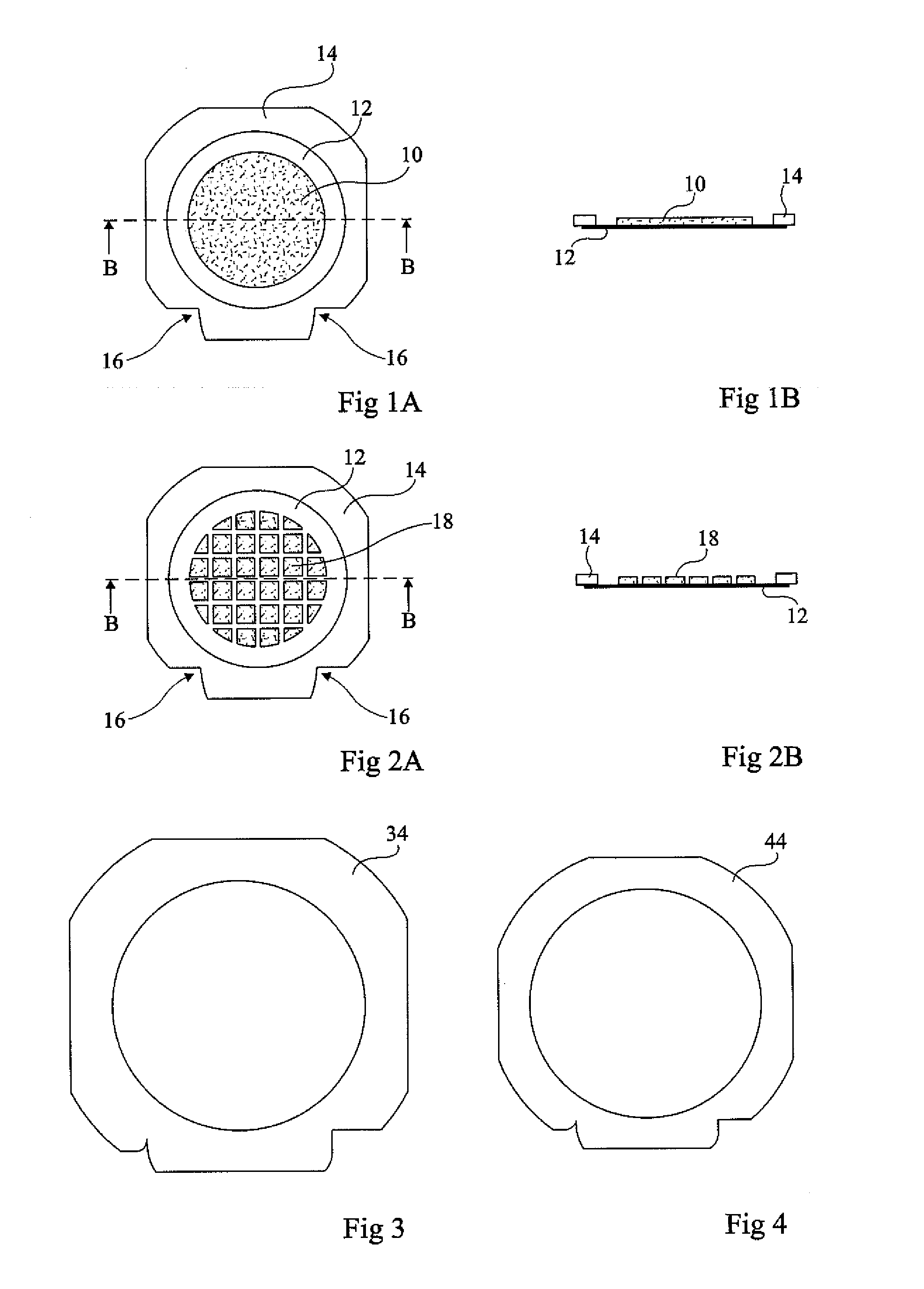
CROSS REFERENCE TO RELATED APPLICATIONS[0001]This application claims the priority benefit of French patent application number 10 / 54472, filed on Jun. 8, 2010, entitled “METHOD FOR MANUFACTURING SEMICONDUCTOR CHIPS FROM A SEMICONDUCTOR WAFER,” which is hereby incorporated by reference to the maximum extent allowable by law.BACKGROUND OF THE INVENTION[0002]1. Field of the Invention[0003]The present invention relates to a method for manufacturing semiconductor chips from a semiconductor wafer.[0004]2. Discussion of the Related Art[0005]The manufacturing of semiconductor chips especially comprises steps during which components and interconnect metallizations are formed inside and on top of a semiconductor wafer, followed by a step during which the wafer is cut into individual chips, for example, by means of a saw. Various individual chip testing steps are generally provided after the cutting.[0006]FIGS. 1A, 1B and 2A, 2B schematically illustrate steps of a method for cutting a semicondu...

Claims


Application Information

Patent Timeline
IPC IPC(8): H01L21/66H01L21/683
CPCH01L21/78H01L21/67132H01L21/683Y10T29/41Y10T225/393Y10T83/02
Inventor JARRY, VINCENTHOUGRON, PATRICKTOUZET, DOMINIQUEMENDEZ, JOSE
Owner STMICROELECTRONICS (TOURS) SAS
Learn More