Light-emitting device and projector

Inactive Publication Date: 2011-12-15
SEIKO EPSON CORP
View PDF2 Cites 4 Cited by
  • Summary
  • Abstract
  • Description
  • Claims
  • Application Information

AI Technical Summary

Benefits of technology

[0030]In this projector, it is possible to obtain h

Problems solved by technology

Particularly, when InGaN is used in the light-emitting layer and materials other than InGaN (for example, GaN) are used in the substrate, lattice mismatch therebetween is generated and the strain increases.
Therefore, non-radiative recombination caused by an impurity or a defect near the side surface occurs, and light-e

Method used


Image

  • Light-emitting device and projector
  • Light-emitting device and projector
  • Light-emitting device and projector

Examples


Example

[0045]Hereinafter, preferable embodiments of the invention will be described with reference to the accompanying drawings.

1. Light-Emitting Device

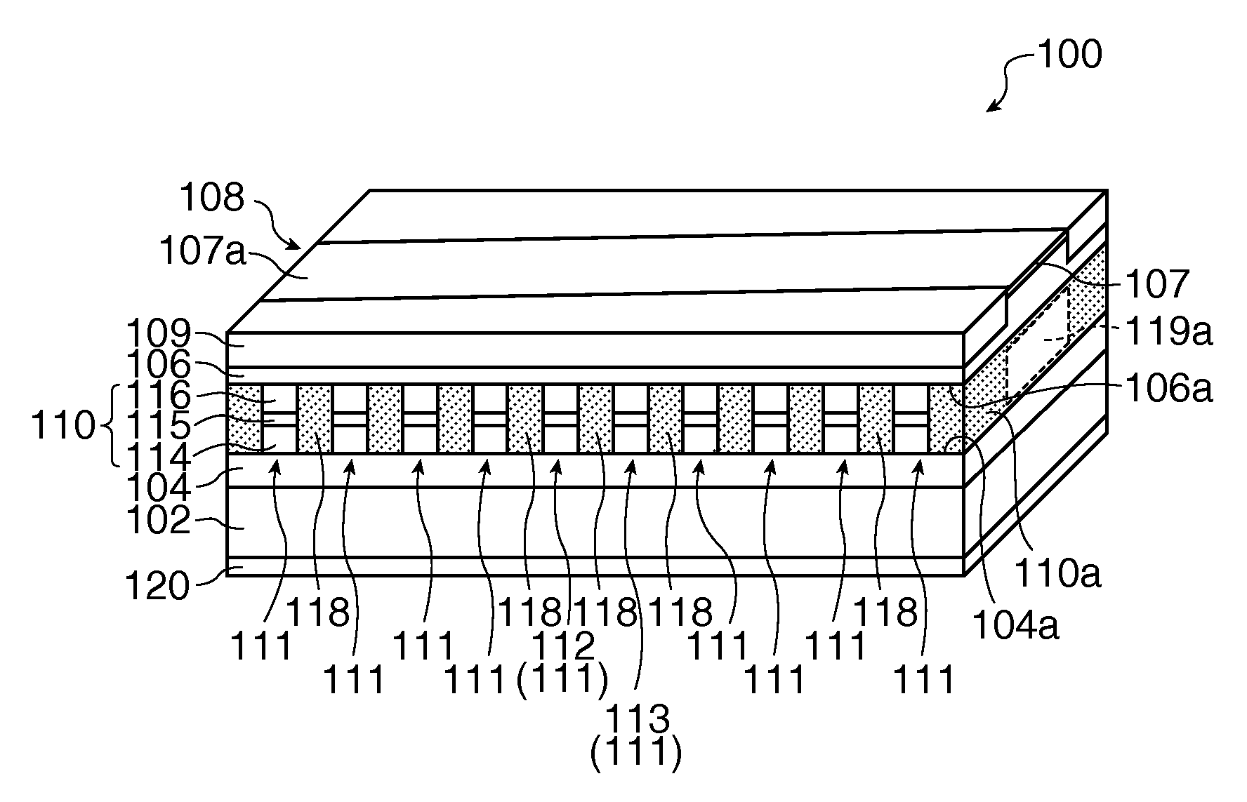
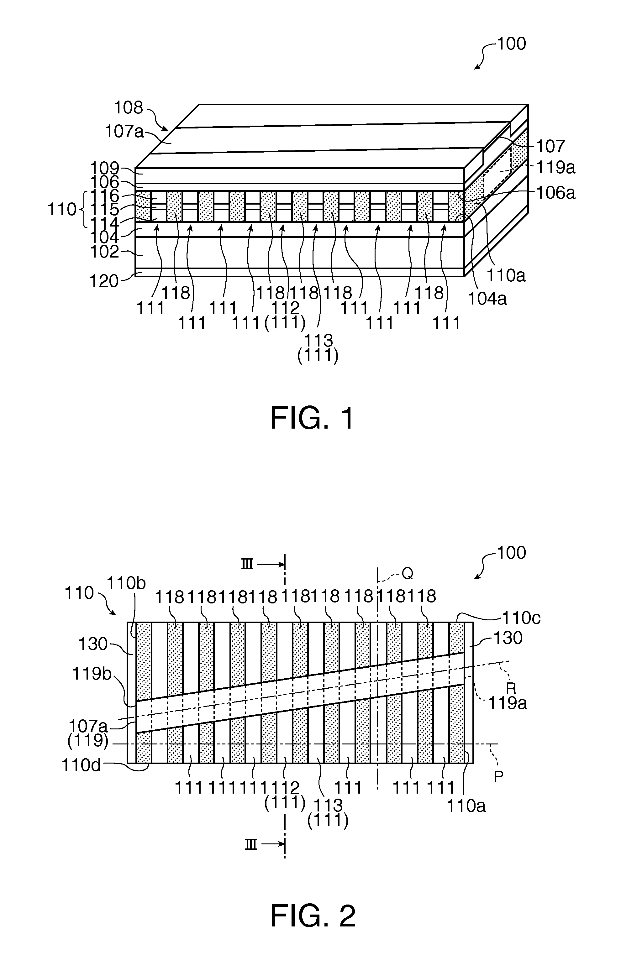
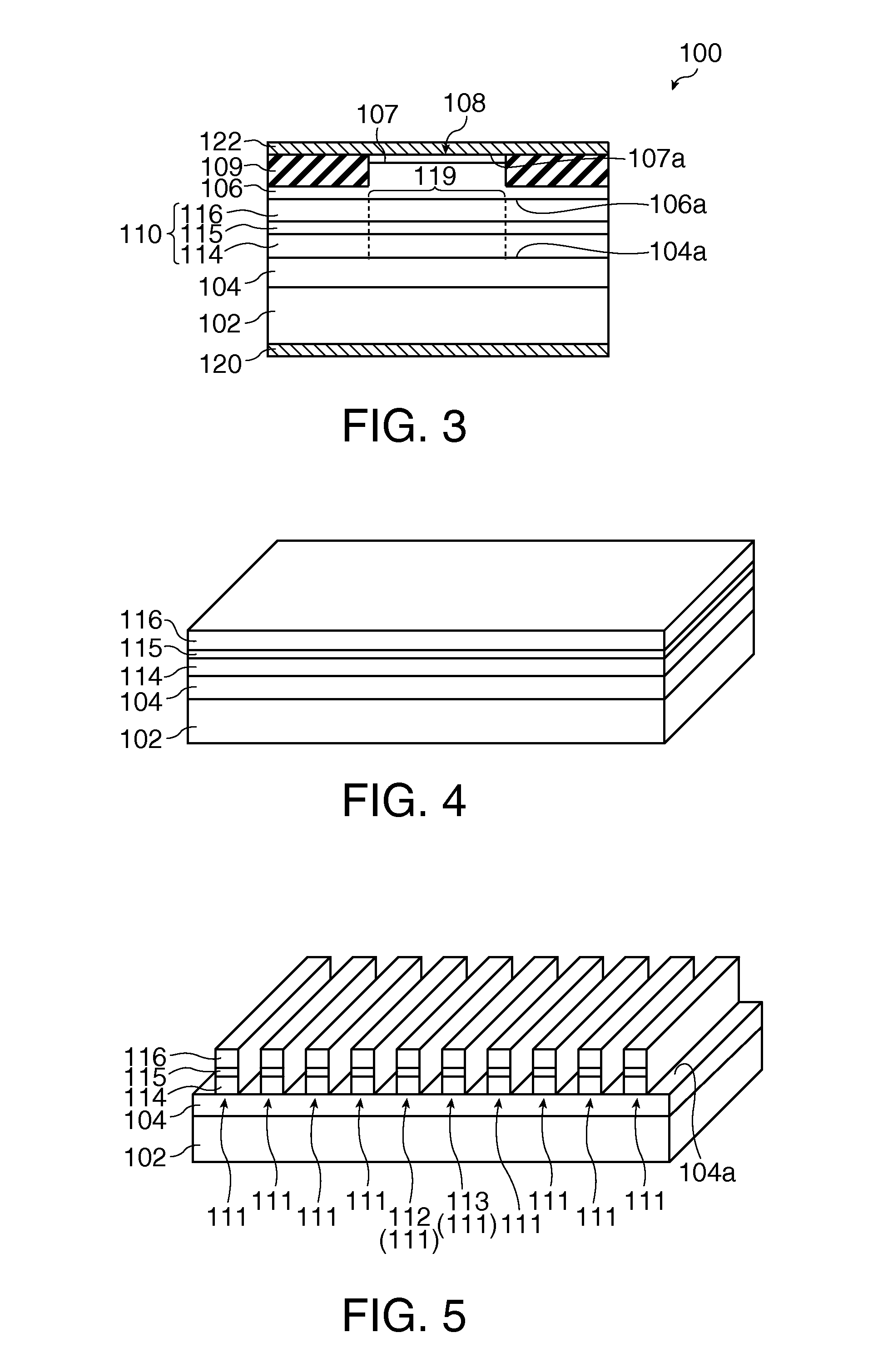
[0046]First, a light-emitting device according to an embodiment of the invention will be described with reference to the accompanying drawings. FIG. 1 is a perspective view schematically illustrating a light-emitting device 100 according to an embodiment of the invention. FIG. 2 is a plan view schematically illustrating the light-emitting device 100 according to the embodiment of the invention. FIG. 3 is a cross-sectional view taken along the line of FIG. 2 for schematically illustrating the light-emitting device 100 according to the embodiment of the invention. In addition, in FIG. 1, a second electrode 122 and a sixth layer 130 are omitted for the sake of convenience. In addition, in FIG. 2, a second layer 106, an insulating portion 109, and a second electrode 122 are omitted for the sake of convenience.

[0047]As an example, a case where a...


PUM


Abstract

A light-emitting device includes a first layer, a second layer, and a semiconductor body interposed between the first and second layers, wherein the semiconductor body has a first fine-wall-shape member, a second fine-wall-shape member, and a semiconductor member interposed between the first and second fine-wall-shape members, the first and second fine-wall-shape members have a third layer, a fourth layer, and a fifth layer interposed between the third and fourth layers, the fifth layer is a layer that generates light and guides the light, the third and fourth layers are layers that guide the light generated in the fifth layer, and the first and second layers are layers that suppress leakage of the light generated in the fifth layer.

Description

BACKGROUND[0001]1. Technical Field[0002]The present invention relates to a light-emitting device and a projector.[0003]2. Related Art[0004]There is known a light-emitting device obtained by forming a light-emitting layer made of a group-III nitride semiconductor on a substrate, injecting a current from an external portion, and combining electrons and holes inside the light-emitting layer so as to emit light. In such a light-emitting device, a strain may be generated between a light-emitting layer and a substrate. Particularly, when InGaN is used in the light-emitting layer and materials other than InGaN (for example, GaN) are used in the substrate, lattice mismatch therebetween is generated and the strain increases. When such the strain is generated, an electric field due to a piezoelectric effect (piezoelectric field) is applied to the light-emitting layer, and a radiative recombination probability between electrons and holes is noticeably reduced.[0005]In order to address the afor...

Claims


Application Information

Patent Timeline
IPC IPC(8): H01L33/06
CPCG03B21/14H01L33/0045H04N9/3197H01L33/32H04N9/315H01L33/08G03B21/2033
Inventor MOCHIZUKI, MASAMITSU
Owner SEIKO EPSON CORP
Why Eureka
Try Eureka