

Photoelectric conversion device
- Summary
- Abstract
- Description
- Claims
- Application Information
AI Technical Summary
Benefits of technology
Problems solved by technology
Method used
Image

Examples
embodiment 1
[0035]In this embodiment, a photoelectric conversion device according to one embodiment of the present invention, and a manufacturing method thereof will be described.
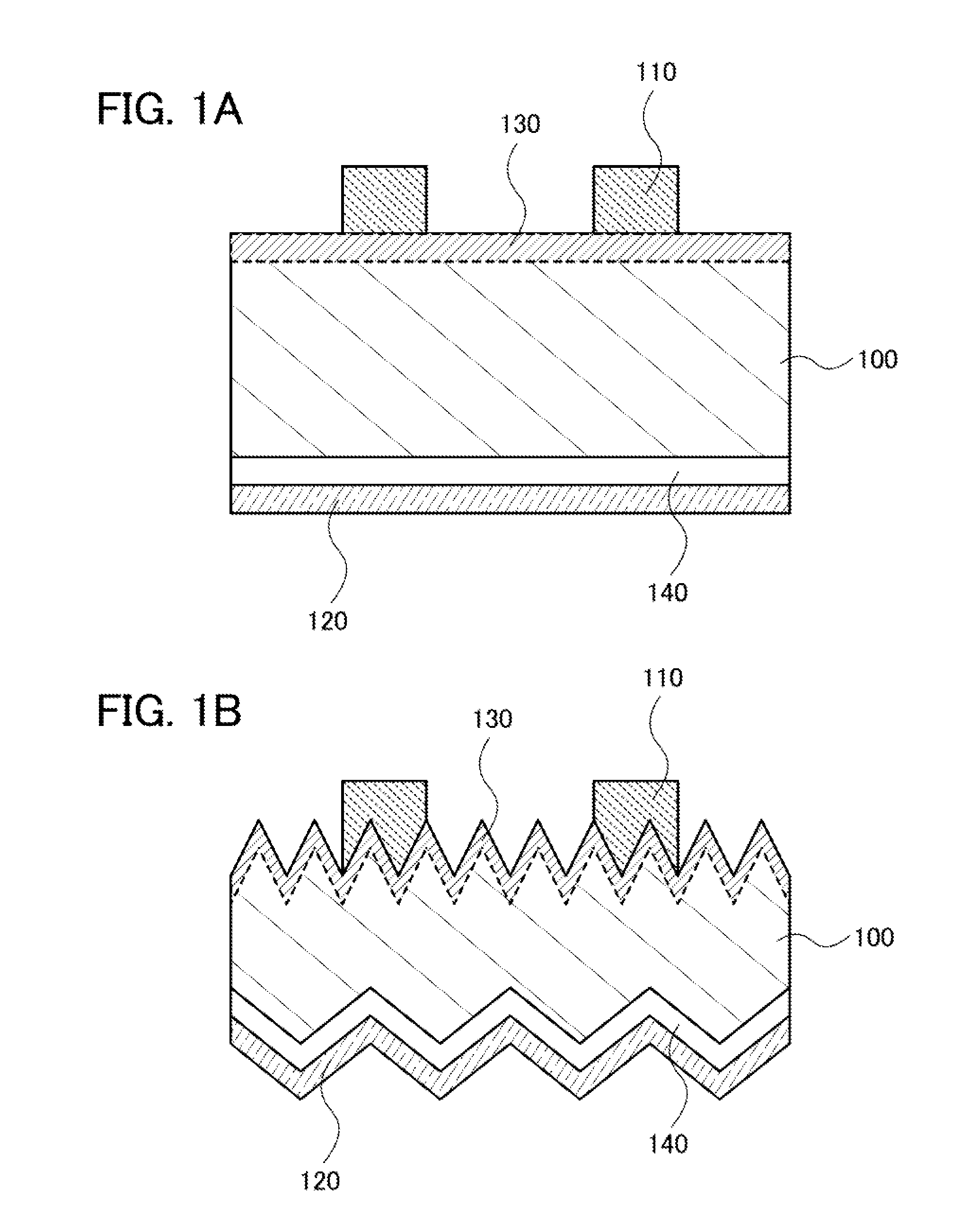
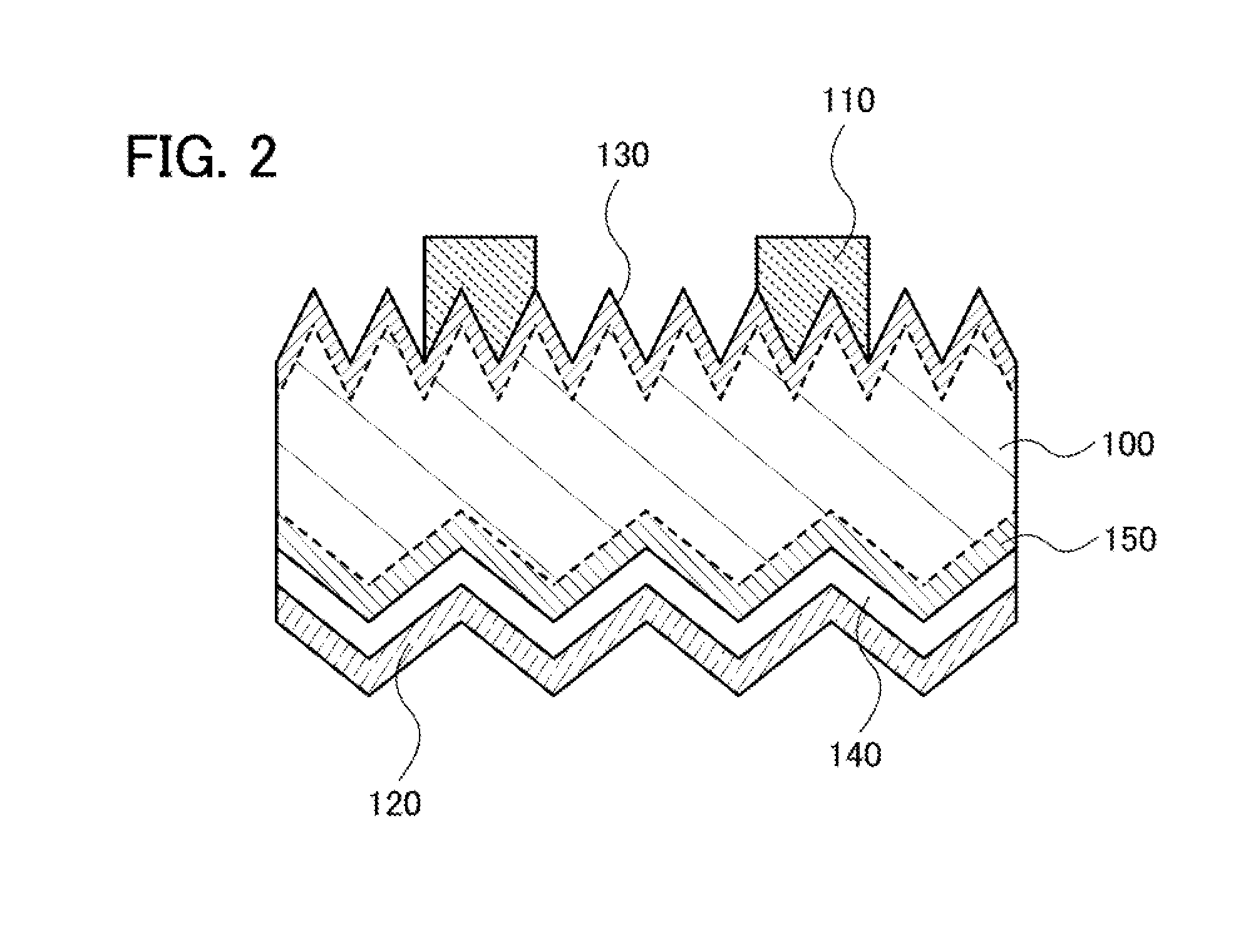
[0036]In recent years, a photoelectric conversion device including a thin crystalline silicon substrate has been desired in view of resource saving and cost reduction. In a photoelectric conversion device, a surface (front surface) and / or a back surface (rear surface) serving as a light-receiving surface are / is provided with unevenness, whereby the electric characteristics can be improved. However, when a crystalline silicon substrate is made thin, the optical path length in the substrate is shortened; thus, among advantageous effects derived from the unevenness provided for the surface of the substrate, an effect of an increase in optical path length is reduced. In order to compensate for this phenomenon, the reflectance of a back electrode is preferably improved.
[0037]In the case where the crystalline silicon substra...
embodiment 2
[0068]In this embodiment, a photoelectric conversion device which has a different structure from that of the photoelectric conversion device described in Embodiment 1, and a manufacturing method thereof will be described.
[0069]FIGS. 3A and 3B each illustrate a cross-sectional view of a photoelectric conversion device according to one embodiment of the present invention.
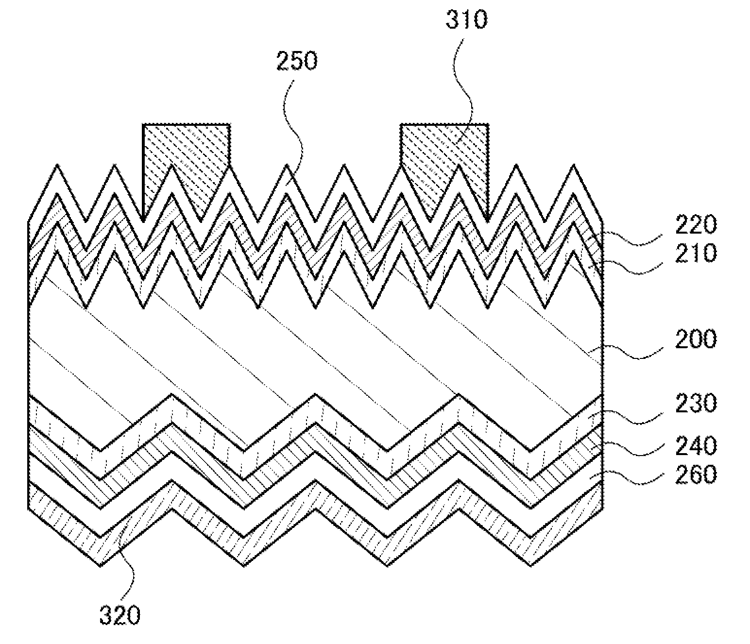
[0070]A photoelectric conversion device illustrated in FIG. 3A includes a first semiconductor layer 210 formed on one surface of a crystalline silicon substrate 200, a second semiconductor layer 220 formed on the first semiconductor layer, a first light-transmitting conductive film 250 formed on the second semiconductor layer, a first electrode 310 formed on the first light-transmitting conductive film, a third semiconductor layer 230 formed on the other surface of the crystalline silicon substrate 200, a fourth semiconductor layer 240 formed on the third semiconductor layer 230, a second light-transmitting conductive...
embodiment 3
[0098]In this embodiment, the light-transmitting conductive film described in Embodiments 1 and 2 will be described.
[0099]As the light-transmitting conductive film used as a reflection layer of the photoelectric conversion device described in Embodiments 1 and 2, a composite material of a transition metal oxide and an organic compound can be used. Note that in this specification, the word “composite” means not only a state in which two materials are simply mixed but also a state in which a plurality of materials is mixed arid charges are transferred between the materials.
[0100]As the transition metal oxide, a transition metal oxide having an electron-accepting property can be used. Specifically, among transition metal oxides, an oxide of a metal belonging to any of Groups 4 to 8 of the periodic table is preferable. In particular, vanadium oxide, niobium oxide, tantalum oxide, chromium oxide, molybdenum oxide, tungsten oxide, manganese oxide, and rhenium oxide are preferable because ...
PUM
 Abstract
Description
Claims
Application Information