Display device and method for manufacturing the same

a technology of a display device and a manufacturing method, which is applied in the direction of semiconductor devices, electrical devices, transistors, etc., can solve the problems of remarkably increasing surface roughness of the organic insulating layer, and achieve the effect of effective annealing and effective manufacturing

Active Publication Date: 2011-12-15
SAMSUNG DISPLAY CO LTD
View PDF6 Cites 28 Cited by
  • Summary
  • Abstract
  • Description
  • Claims
  • Application Information

AI Technical Summary

Benefits of technology

[0035]According to exemplary embodiments, the display device can prevent an internal short-circuit.
[0036]Furthermore, the semiconductor layer of t

Problems solved by technology

However, the surface roughness of the organic insulating layer remarkably increases when the

Method used


Image

  • Display device and method for manufacturing the same
  • Display device and method for manufacturing the same
  • Display device and method for manufacturing the same

Examples


Embodiment Construction

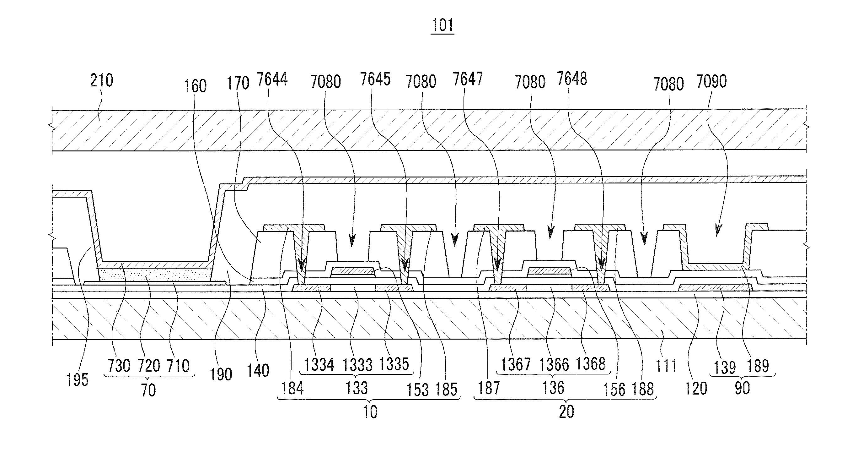
[0045]Most flat panel display devices such as organic light emitting diode (OLED) displays and liquid crystal displays (LCDs) use an organic insulating layer with a thin film transistor. The organic insulating layer is exposed to many etching processes when contact holes are formed or conductive layers are patterned. However, the surface roughness of the organic insulating layer remarkably increases when the organic insulating layer is exposed to an etching process, particularly a dry etching process. If a conductive layer is formed on the organic insulating layer with increased surface roughness and patterned, the conductive material of the conductive layer is easily left on the surface of the organic insulating layer. The conductive material left on the organic insulating layer blocks conductive wires from being electrically insulated from each other so as to cause a short-circuit.

[0046]The present invention will be described more fully hereinafter with reference to the accompanyi...


PUM


Abstract

A display device and a manufacturing method thereof are provided. The display device includes a substrate, a semiconductor layer formed on the substrate, an organic insulating layer formed on the semiconductor layer, a plurality of conductive wires formed on the organic insulating layer. The organic insulating layer has an open groove that is formed between the conductive wires.

Description

CLAIM OF PRIORITY[0001]This application makes reference to, incorporates the same herein, and claims all benefits accruing under 35 U.S.C. §119 from an application earlier filed in the Korean Intellectual Property Office on 9 Jun. 2010 and there duly assigned Serial No. 10-2010-0054407.BACKGROUND OF THE INVENTION[0002]1. Field of the Invention[0003]The described technology relates generally to a display device and a manufacturing method thereof. More particularly, the described technology relates generally to a display device and a manufacturing method thereof for improving the performance of the display device and suppressing the generation of defects in the display device.[0004]2. Description of the Related Art[0005]Most flat panel display devices such as organic light emitting diode (OLED) displays and liquid crystal displays (LCDs) use an organic insulating layer with a thin film transistor.[0006]The organic insulating layer is exposed to many etching processes when contact hole...

Claims


Application Information

Patent Timeline
IPC IPC(8): H01L29/786H01L21/283
CPCH01L27/3246H01L27/3248H01L27/1248H01L27/1288H01L2227/323H10K59/123H10K59/122H10K59/1201H10K59/10
Inventor CHO, KYU-SIKCHOI, JOON-HOOCHOI, BO-KYUNGMOON, SANG-HO
Owner SAMSUNG DISPLAY CO LTD
Why Eureka
Try Eureka