Laser irradiation method and laser irradiation device and method of manufacturing semiconductor device

a laser irradiation and laser irradiation technology, applied in the direction of semiconductor lasers, manufacturing tools, metal working devices, etc., can solve the problems of complicated optical system for forming linear beams, device enlargement, difficult optical adjustment to such an optical system, etc., to achieve convenient optical adjustment, compact size, and simplified configuration

Inactive Publication Date: 2006-09-28
SEMICON ENERGY LAB CO LTD
View PDF76 Cites 12 Cited by
  • Summary
  • Abstract
  • Description
  • Claims
  • Application Information

AI Technical Summary

Benefits of technology

[0014] Hence, an object of the present invention is to provide a laser irradiation device in which a linear beam is formed using an optical system more simplified than the conventional ones and which can effectively anneal using such a linear beam, and a laser irradiation method using such a laser irradiation device. Moreover, another object of the present invention is to provide a method of manufacturing a semiconductor device in which the foregoing laser irradiation method is included in its step.
[0021] Moreover, in the configurations described above, for the foregoing substrate, a glass substrate, a quartz substrate, a silicon substrate, a plastic substrate, a metal substrate, a stainless clad substrate, a flexible substrate and the like can be utilized. As the foregoing glass substrate, a substrate consisted of glass such as barium borosilicate glass, aluminoborosilicate glass or the like can be listed. Moreover, a flexible substrate is referred to a substrate in a film shape consisted of PET, PES, PEN, acryl or the like, if a semiconductor device is prepared by utilizing the flexible substrate, the weight lightening of it is expected. If on the surface or on the surface and the back surface of the flexible substrate, a barrier layer made of aluminum film (AlON, AlN, AlO or the like), carbon film (DLC (diamond like carbon) or the like), SiN or the like is formed in a monolayer or multilayer, it is desirable that the durability or the like is enhanced.
[0027] Moreover, in the respective configurations, it is desirable that the foregoing semiconductor film is a film containing silicon. Since the present invention has a very simplified configuration, optical adjustment is easy, and the device becomes compact in size. Moreover, even in the case where the irradiation is performed using a plurality of laser beams, since the optical system is simplified, it is possible to easily make the same shape of the all laser beams. In order to perform the uniform annealing, it is very important to make the same shape of plurality of laser beams. If the beam irradiates on a substrate having a large area using such a plurality of laser beams, it is capable of enhancing the throughput. Moreover, the beam can be utilized by synthesizing such a plurality of lasers. Furthermore, since the present invention is slantly incident with respect to the irradiated body, the return beam can be prevented, since an isolator is not required to set, the configuration becomes more simplified. Therefore, the reduction of the cost can be realized. Moreover, the efficient irradiation can be performed with respect to the semiconductor film formed on the substrate, and it makes possible that the variation of the electrical property of TFT prepared can be reduced using such a semiconductor. Then, the operating property and reliability of semiconductor prepared from such a TFT can be also enhanced.

Problems solved by technology

However, as shown in FIG. 7, an optical system for forming a linear beam is complicated.
There are problems that it is very difficult to perform optical adjustment to such an optical system, and in addition, since the footprint becomes larger, the device is enlarged.
The return beam becomes a factor having a bad influence on an output of the laser and the variation of frequencies and the destruction of the rod or the like.

Method used


Image

  • Laser irradiation method and laser irradiation device and method of manufacturing semiconductor device
  • Laser irradiation method and laser irradiation device and method of manufacturing semiconductor device
  • Laser irradiation method and laser irradiation device and method of manufacturing semiconductor device

Examples


embodiments

Embodiment 1

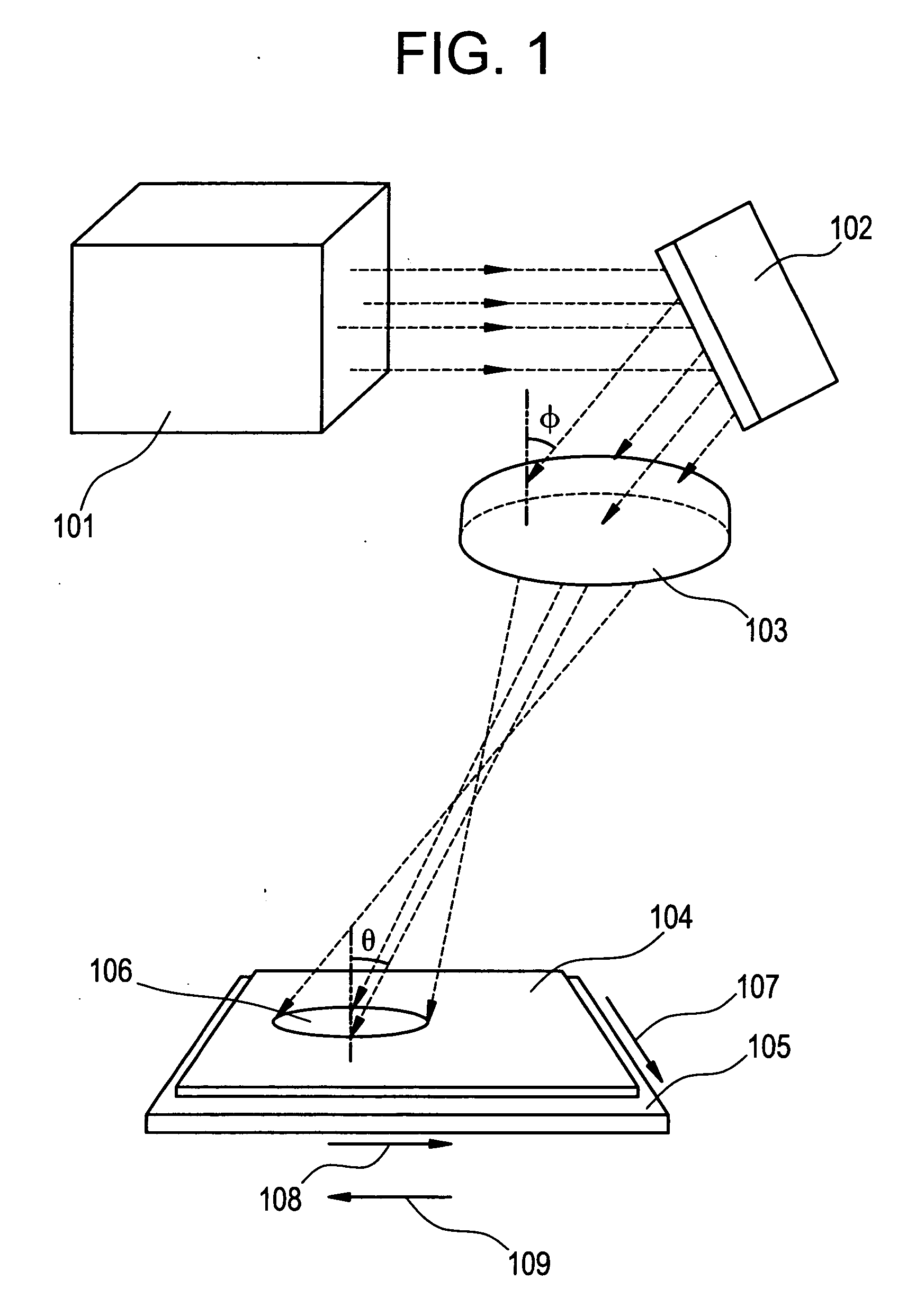
[0067] In the present Embodiment, an example in which a linear beam is formed by the present invention will be described below with reference to FIG. 1 and FIG. 3.

[0068] As the laser 101, YAG laser is used. Supposing that the laser beam oscillated from the laser 101 is converted to the second higher harmonic wave by a non-linear optical element contained in the laser 101. At this time, supposing that the laser beam is in TEMoo mode, and has 2.25 mm of beam diameter and 0.35 mrad of spreading angle.

[0069] Subsequently, the beam is incident with respect to the convex lens 103 having a focal length of 20 mm at the incident angle φ of 20 degrees. Then, in the present Embodiment, the simulation is performed on the shape of the laser beam formed on the irradiation surface disposed in parallel with the convex lens. The results of these are shown in FIG. 3. From FIG. 3, it is understood that a linear beam having a length of 420 μm and a width of 40 μm is formed on the irradia...

embodiment 2

[0071] In the present Embodiment, an example in which the irradiation of the laser beam is performed using a plurality of laser beams will be described below with reference to FIG. 4. As lasers 111a-111c, YAG lasers are used, these are converted into the second higher harmonic wave by a non-linear optical element. Then, after the respective laser beams emitted from the lasers 111a-111c travel via mirrors 112a-112c, these are slantly incident with respect to the convex lenses 113a-113c. By slantly being incident, the focal position is shifted by an aberration such as astigmatism or the like, a linear beam can be formed on the irradiation surface or in its neighborhood. Moreover, it is desirable that an aspherical lens is used for the convex lens. It should be noted that abeam expander between the lasers 111a-111c and the mirrors 112a-112c or between the mirrors 112a-112c and the convex lenses 113a-113c is set and may be expanded into the desired sizes in both of longer direction and ...

embodiment 3

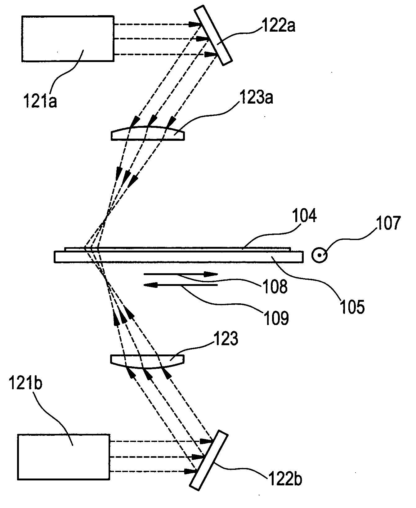
[0075] In the present Embodiment, an example in which the irradiation of the laser beams are carried out from both sides of the irradiated body using a plurality of lasers will be described below with reference to FIG. 5.

[0076] As lasers 121a, 121b, YVO4 lasers of continuous oscillation are used, these are converted into the second higher harmonic wave by utilizing a non-linear optical element. Then, after the respective laser beams emitted from the lasers 121a,121b travel via mirrors 122a,122b, these are slantly incident with respect to the convex lenses 123a,123b. By slantly being incident, the focal position is shifted by an aberration such as astigmatism or the like, a linear beam can be formed on the irradiation surface or in its neighborhood. Moreover, it is desirable that an aspherical lens is used for the convex lens.

[0077] It should be noted that a beam expander between the lasers 121a, 121b and the mirrors 122a, 122b or between the mirrors 122a, 122b and the convex lense...


PUM

PropertyMeasurementUnit
lengthaaaaaaaaaa
aspect ratioaaaaaaaaaa
sizeaaaaaaaaaa

Abstract

The present invention is characterized in that by laser beam being slantly incident to the convex lens, an aberration such as astigmatism or the like is occurred, and the shape of the laser beam is made linear on the irradiation surface or in its neighborhood. Since the present invention has a very simple configuration, the optical adjustment is easier, and the device becomes compact in size. Furthermore, since the beam is slantly incident with respect to the irradiated body, the return beam can be prevented.

Description

BACKGROUND OF THE INVENTION [0001] 1. Field of the Invention [0002] The present invention relates to a laser irradiation method and a laser irradiation apparatus for using the method (apparatus including a laser and an optical system for guiding laser beam emitted from the laser to an object to be irradiated). In addition, the present invention relates to a method of manufacturing a semiconductor device, which includes a laser beam irradiation step. Note that a semiconductor device described here includes an electro-optical device such as a liquid crystal display device or a light emitting device and an electronic device which includes the electro-optical device as a part. [0003] 2. Description of the Related Art [0004] In recent years, a wide study has been made on a technique in which laser annealing is performed for a semiconductor film formed on an insulating substrate made of glass or the like, to crystallize the film, to improve its crystallinity so that a crystalline semicond...

Claims


Application Information

Patent Timeline
Patent Type & Authority Applications(United States)
IPC IPC(8): H01S5/00H01L21/20B23K26/073H01L21/265H01L21/268H01L21/336H01L21/77H01L21/84H01L29/786H01S3/00H01S3/10
CPCB23K26/0604B23K26/0608B23K26/0732B23K26/0736B23K26/0738B23K2201/40H01L27/1285H01L27/1296H01L27/14625H01L21/02532H01L21/02592H01L21/02675H01L21/268H01L21/283B23K26/352B23K2101/40H01S3/10
Inventor TANAKA, KOICHIROMIYAIRI, HIDEKAZUSHIGA, AIKOSHIMOMURA, AKIHISAISOBE, ATSUO
Owner SEMICON ENERGY LAB CO LTD
Why Eureka
Try Eureka