

Image display device, driving method of image display device and terminal device
- Summary
- Abstract
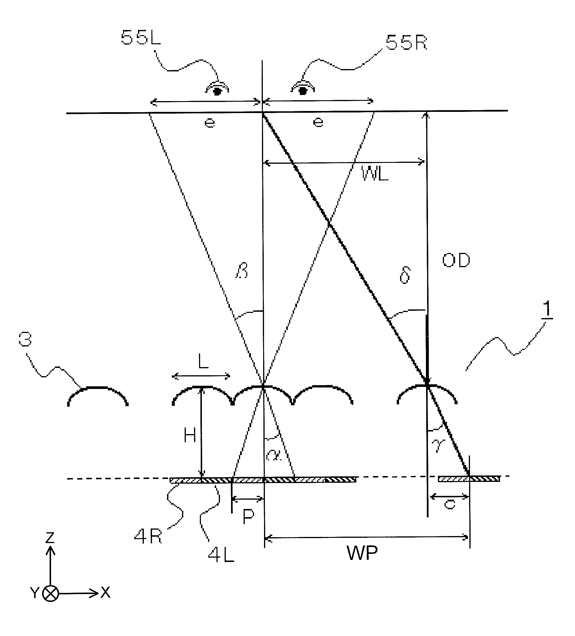
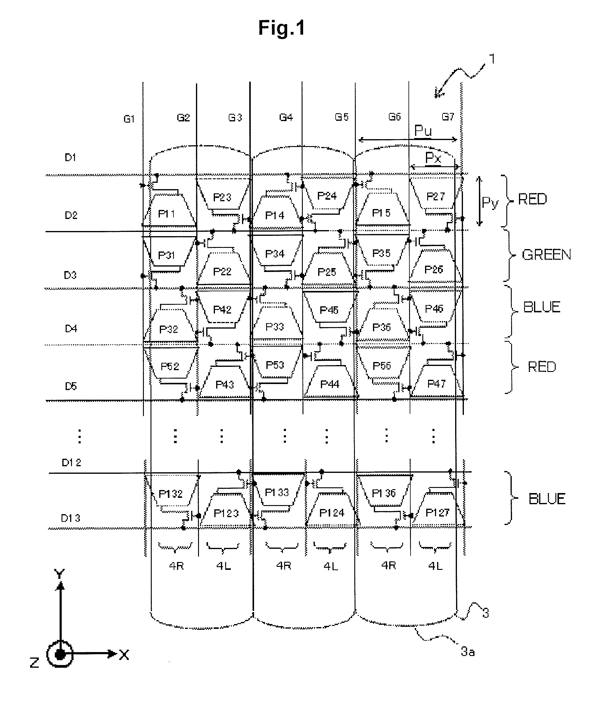
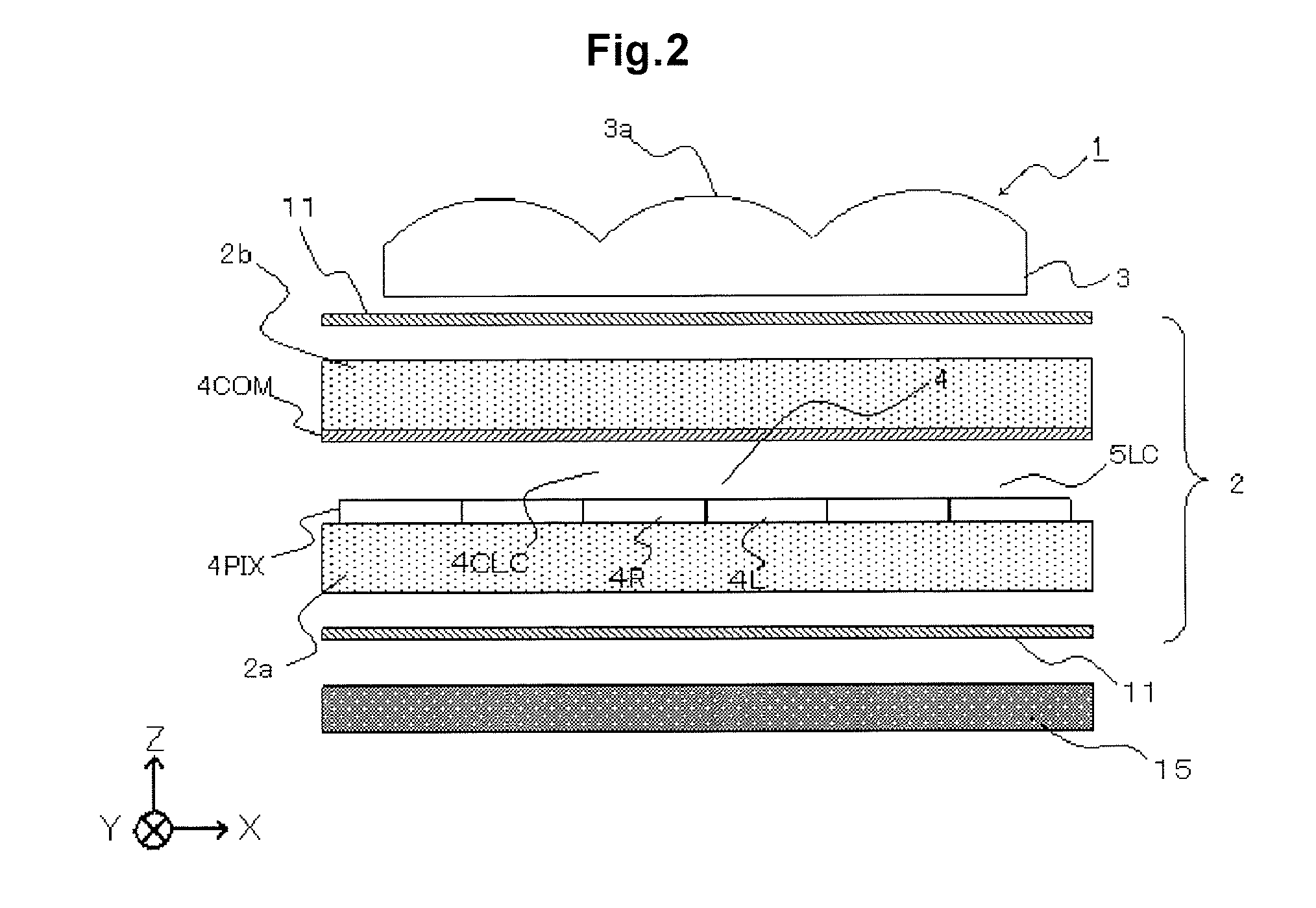
- Description
- Claims
- Application Information
AI Technical Summary
Benefits of technology
Problems solved by technology
Method used
Image

Examples
first exemplary embodiment
Modified Example of First Exemplary Embodiment
[0210]Next, an explanation will be given of a first modified example of the first exemplary embodiment.
[0211]FIG. 17 is a plan view of a display panel 2 according to a first modified example of the first exemplary embodiment. As shown in FIG. 17, a storage capacitor line CS is arranged so as to traverse a pixel aperture, and an end of a black matrix 60 is inclined from the image separating direction at a location where the black matrix 60 contacts the storage capacitor line CS. The inclination angle of the black matrix 60 at a region X12 satisfies a condition in which |θ1|=|φ1|=|φ′1|=φ2|=|φ′2|. Hence, the vertical aperture ratio in the X axis direction is made constant at a region X1, so that 3D moire originating from the storage capacitor line CS can be reduced.
[0212]The configuration and the operation other than the above-explained configuration and operation are same as those of the first exemplary embodiment.
[0213]Next, an explanatio...
second exemplary embodiment
[0240]Next, an explanation will be given of a second exemplary embodiment of the present invention. FIGS. 23 and 24 are plan views showing an image display device according to the present exemplary embodiment. Regarding the pixels adjoining in the Y axis direction, i.e., the adjoining pixel pair in the present exemplary embodiment, in comparison with that of the first exemplary embodiment, the directions of respective storage capacitor lines CS passing all the way through the aperture are nonparallel, and are inclined in directions different from the image separating direction. Moreover, regarding the pixels adjoining in the X axis direction, i.e., the right and left pixels configuring a unit of display, the directions of respective storage capacitor lines CS passing all the way through the aperture are nonparallel, and are inclined in directions different from the image separating direction.
[0241]The pixel matrix of the present exemplary embodiment has the pixels shown in FIGS. 23 ...
third exemplary embodiment
[0247]Next, an explanation will be given of a third exemplary embodiment of the present invention. FIGS. 25 and 26 are plan views showing a pixel structure of an image display device according to the present exemplary embodiment, and FIG. 27 is a plan view showing a display panel 2 according to the third exemplary embodiment.
[0248]In comparison with the first exemplary embodiment, in the present exemplary embodiment, a pixel shape is changed from a substantially trapezoidal shape to a substantially octagonal shape.
[0249]The pixel is formed in a substantially octagonal shape having a substantially trapezoidal pixel cut through a virtual section line interconnecting the upper bottom and the lower bottom and divided into two right trapezoids, each of the two right trapezoids is shifted in the +Y direction and in −Y direction by a predetermined size, and cut portions are connected together. As shown in FIG. 27, a region X1 is divided into three regions so that X1=X′1+2×X4, and the stora...
PUM
 Abstract
Description
Claims
Application Information