Simultaneous Testing of Semiconductor Components on a Wafer

a technology of semiconductor components and semiconductor wafers, applied in automated test systems, testing circuits, instruments, etc., can solve the problems of increasing the overall size and cost of conventional automatic test equipment, and one or more semiconductor components to operate differently

Inactive Publication Date: 2011-12-22
AVAGO TECH INT SALES PTE LTD
View PDF5 Cites 29 Cited by
  • Summary
  • Abstract
  • Description
  • Claims
  • Application Information

AI Technical Summary

Problems solved by technology

However, imperfections within the semiconductor wafer, such as imperfections of the semiconductor substrate, imperfections of the semiconductor device fabrication operation, or imperfections in design of the components themselves, may cause one or more of the semiconductor components to operate differently than expected.
These more complex semiconductor components require more testing points to perform the testing operation which occupy more real estate on the semiconductor substrate that could be allocated elsewhere.
As a result, these improvements in semiconductor device fabrication have led to an increase of the overall size and cost of the conventional automatic test equipment.

Method used


Image

  • Simultaneous Testing of Semiconductor Components on a Wafer
  • Simultaneous Testing of Semiconductor Components on a Wafer
  • Simultaneous Testing of Semiconductor Components on a Wafer

Examples


Embodiment Construction

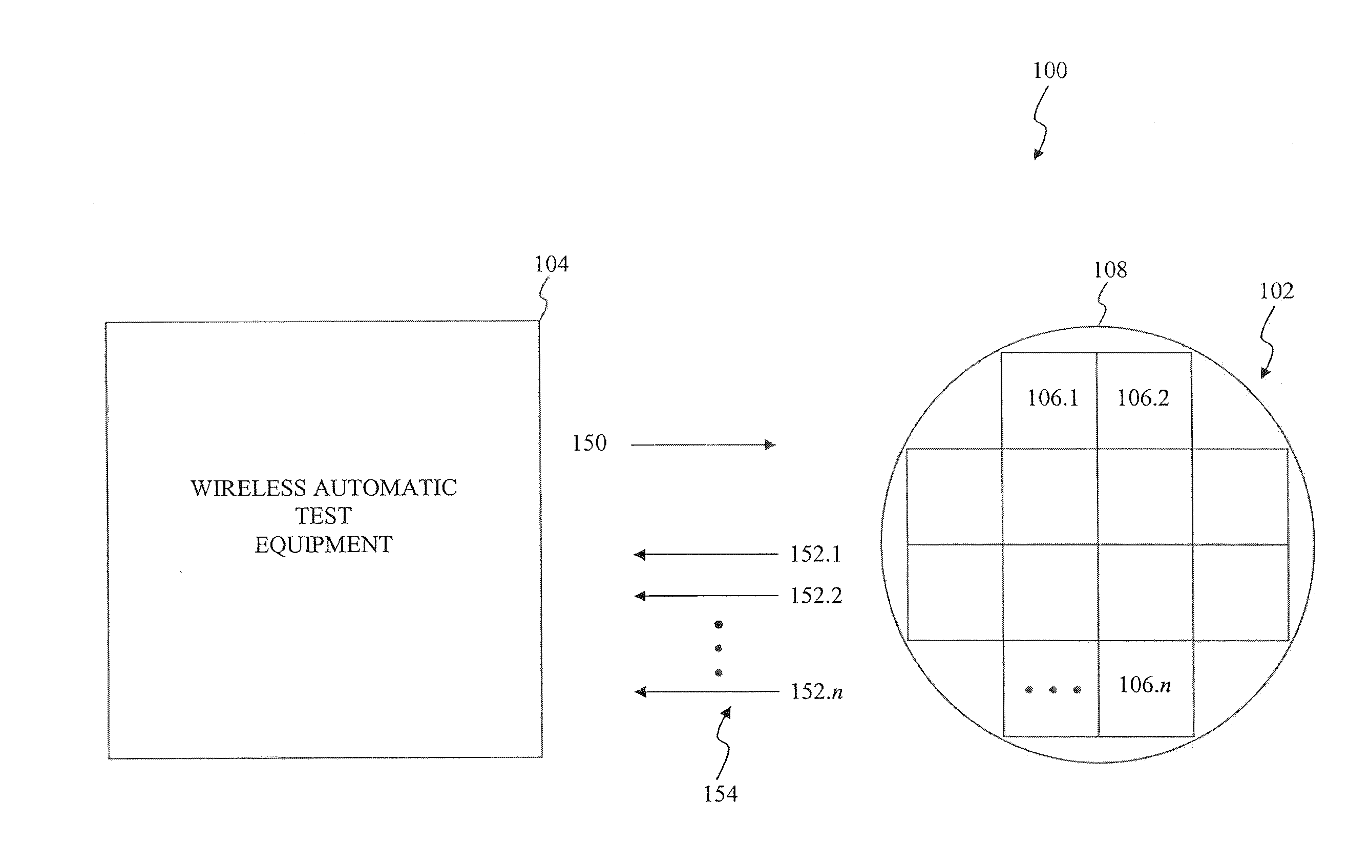
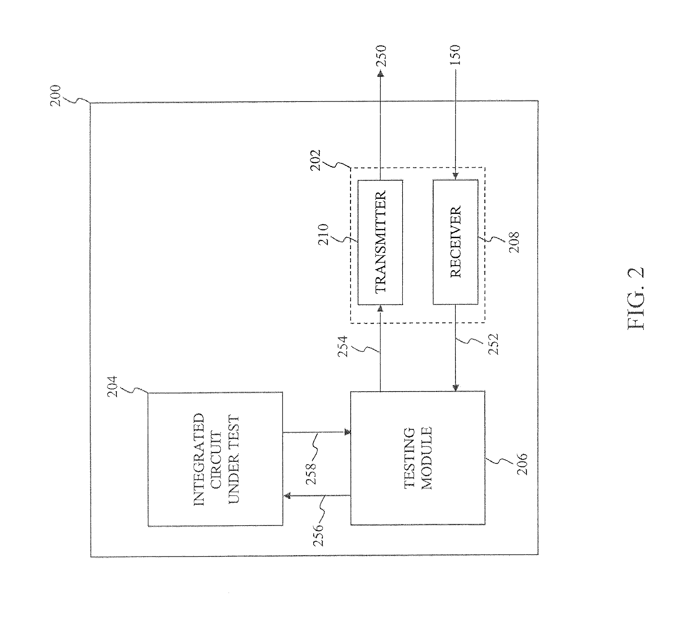
[0032]The following Detailed Description refers to accompanying drawings to illustrate exemplary embodiments consistent with the invention. References in the Detailed Description to “one exemplary embodiment,”“an exemplary embodiment,”“an example exemplary embodiment,” etc., indicate that the exemplary embodiment described may include a particular feature, structure, or characteristic, but every exemplary embodiment may not necessarily include the particular feature, structure, or characteristic. Moreover, such phrases are not necessarily referring to the same exemplary embodiment. Further, when a particular feature, structure, or characteristic is described in connection with an exemplary embodiment, it is within the knowledge of those skilled in the relevant art(s) to effect such feature, structure, or characteristic in connection with other exemplary embodiments whether or not explicitly described.

[0033]The exemplary embodiments described herein are provided for illustrative purp...


PUM


Abstract

Methods and apparatus are disclosed to simultaneously, wirelessly test semiconductor components formed on a semiconductor wafer. The semiconductor components transmit respective outcomes of a self-contained testing operation to wireless automatic test equipment via a common communication channel. Multiple receiving antennas observe the outcomes from multiple directions in three dimensional space. The wireless automatic test equipment determines whether one or more of the semiconductor components operate as expected and, optionally, may use properties of the three dimensional space to determine a location of one or more of the semiconductor components. The wireless testing equipment may additionally determine performance of the semiconductor components by detecting infrared energy emitted, transmitted, and / or reflected by the semiconductor wafer before, during, and / or after a self-contained testing operation.

Description

CROSS-REFERENCE TO RELATED APPLICATIONS[0001]The present application claims the benefit of U.S. Provisional Patent Appl. Nos. 61 / 355,226, filed Jun. 16, 2010, and 61 / 429,277, filed on Jan. 3, 2011, each of which is incorporated herein by reference in its entirety.BACKGROUND[0002]1. Field of Invention[0003]The present invention relates generally to testing of semiconductor components within a semiconductor wafer and specifically to wireless testing of the semiconductor components within the semiconductor wafer simultaneously and, optionally, measuring a performance of the semiconductor components within the semiconductor wafer.[0004]2. Related Art[0005]A semiconductor device fabrication operation is commonly used to manufacture components onto a semiconductor substrate to form a semiconductor wafer. The semiconductor device fabrication operation uses a predetermined sequence of photographic and / or chemical processing steps to form components onto the semiconductor substrate. However,...

Claims


Application Information

Patent Timeline
Patent Type & Authority Applications(United States)
IPC IPC(8): G06F19/00G01R31/26
CPCG01R31/2834G01R31/311G01R31/3025
Inventor BEHZAD, ARYA REZAROFOUGARAN, AHMADREZAZHAO, SAM ZIQUNCASTANEDA, JESUS ALFONSOBOERS, MICHAEL
Owner AVAGO TECH INT SALES PTE LTD
Why Eureka
Try Eureka