Display device and display driving method therefor

a display device and driving method technology, applied in the field of display devices, can solve problems such as difficulty in realizing a large-scale and high-definition display device, and achieve the effects of enhancing the function of mobility correction during bootstrapping operation, and enhancing the ability of mobility correction

Active Publication Date: 2011-12-29
JOLED INC
View PDF1 Cites 0 Cited by
  • Summary
  • Abstract
  • Description
  • Claims
  • Application Information

AI Technical Summary

Benefits of technology

[0013]Here, when the intermediate voltage is written, the operation for writing the intermediate voltage is ended before the voltage at the gate node of the driving transistor reaches the intermediate voltage. As a result, the function of correcting the mobility during the bootstrapping operation is enhanced.
[0014]As set forth hereinabove, according to the present invention, when the two-stage write system is ado

Problems solved by technology

Although the former is simple in configuration, the former involves a problem that it i

Method used


Image

  • Display device and display driving method therefor
  • Display device and display driving method therefor
  • Display device and display driving method therefor

Examples


first embodiment

[1. Configurations of Display Device of First embodiment and Pixel Circuit]

[2. Operation of Pixel Circuit Considered in Course of Reaching the Invention (Comparative Example)]

[0026][3. First example]

[4. Second example]

second embodiment (

[5. Second Embodiment (Display Driving Method for Display Device)]

1. Configurations of Display Device of Embodiments and Pixel Circuit

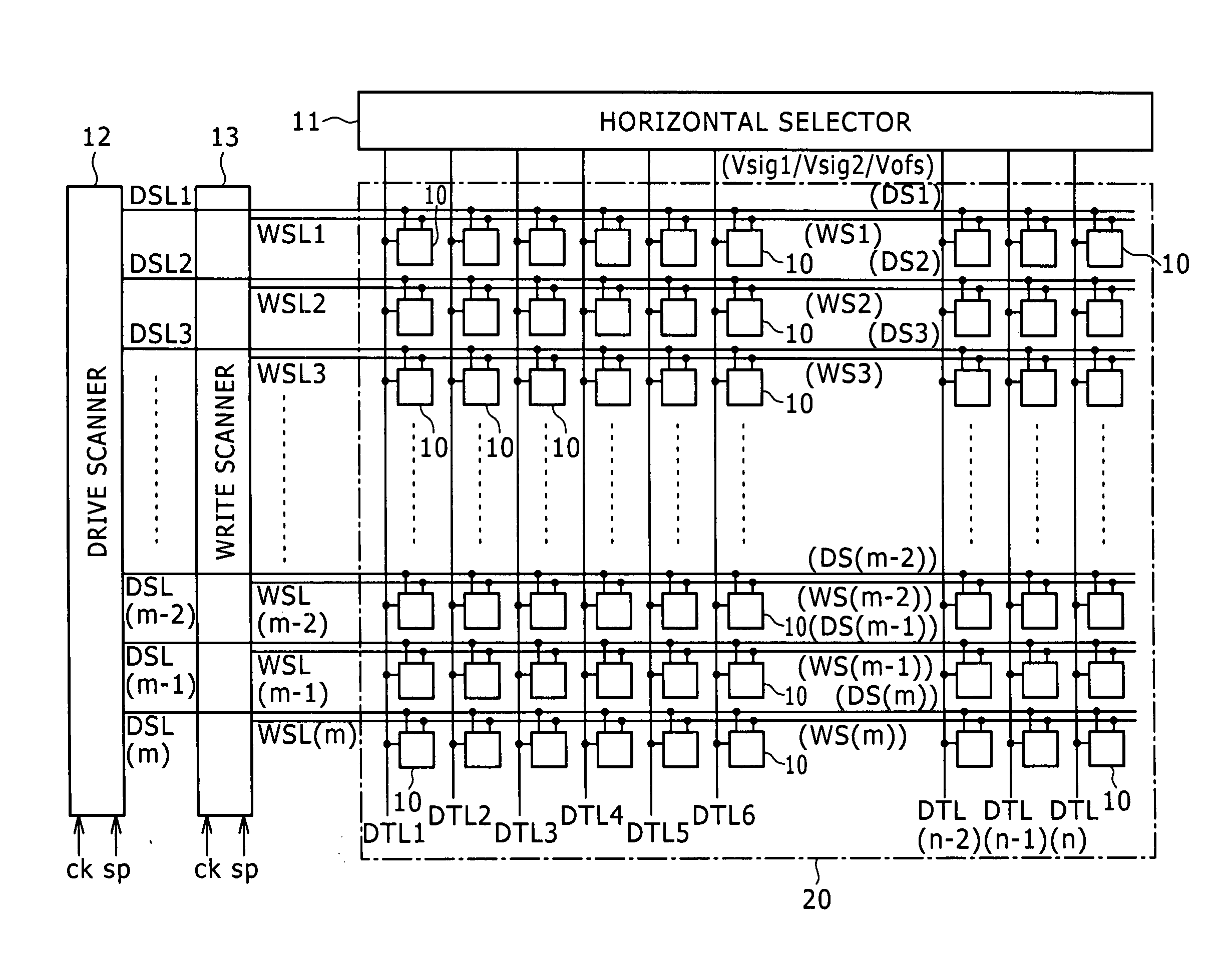
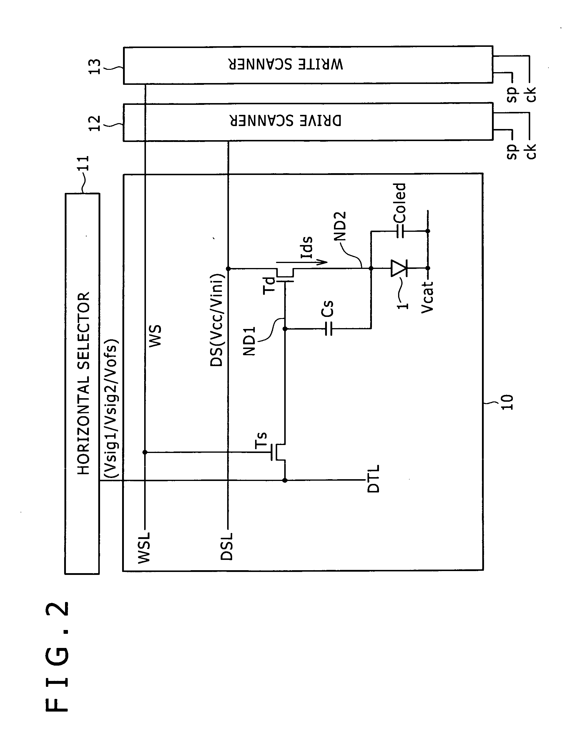
[0027]FIG. 1 shows a configuration of an organic EL display device according to a first embodiment of the present invention.

[0028]The organic EL display device uses an organic EL element as a light emitting element, and includes pixel circuits 10 for carrying out emission drive in accordance with an active matrix system.

[0029]As shown in FIG. 1, the organic EL display device has a pixel array 20 in which a large number of pixel circuits 10 are disposed both in a column direction and in a row direction (m row×n column) in a matrix. It is noted that each of the pixel circuits 10 composes an emission pixel corresponding to any one of Red (R), Green (G) and Blue (B), and the pixel circuits 10 corresponding to R, G and B, respectively, are disposed in accordance with predetermined regulations, thereby configuring a color display device.

[0030]The organic EL...

first example

3. First Example

[0127]Then, in the first embodiment of the present invention, even though the intermediate voltage Vsig1 is not made high, it is possible to cope with the wider mobility dispersion.

[0128]In a first example of the first embodiment, this is realized by shorting the period LT4 of time for which the intermediate voltage Vsig1 is written.

[0129]FIG. 8 shows the voltage of the signal line DTL, the power source pulse DS, the sampling pulse WS, and the voltages at the nodes ND1 and ND2 in the form of a timing chart of the operation for one cycle (one frame period of time) in a certain pixel circuit 10 similarly to the case of FIG. 3.

[0130]Note that, for comparison, with regard to the scanning pulse WS, and the voltages at the nodes ND1 and ND2, the waveforms of FIG. 3 are additionally indicated by chain lines, respectively. In this first example, waveforms of the scanning pulse WS, and the voltages at the nodes ND1 and ND2 are indicated by solid lines, respectively.

[0131]Sinc...


PUM


Abstract

Disclosed herein is a display device, including: a pixel array in which pixel circuits each having a light emitting element, a driving transistor for applying a current corresponding to a gate-to-source voltage to the light emitting element connected to a source side by applying a drive voltage across a drain and a source, a sampling transistor for inputting a signal line voltage to a gate of the driving transistor by being caused to conduct, and a sustaining capacitor connected between the gate and the source of the driving transistor for sustaining a video signal voltage inputted thereto are disposed in a matrix; a signal selector; a drive control scanner; and a write scanner.

Description

BACKGROUND OF THE INVENTION[0001]1. Field of the Invention[0002]The present invention relates to a display device having a pixel array in which pixel circuits are disposed in a matrix, and a display driving method therefor. More particularly, the invention relates to a display device, using an organic electro-luminescence element (organic EL element) as a light emitting element, and a display driving method therefor.[0003]2. Description of the Related Art[0004]An image display device using an organic EL element in a pixel has been developed. Since the organic EL element is a self-emission element, the organic EL element has an advantage that, for example, the visibility of an image is high, a backlight is unnecessary, a response speed is high, and the like as compared with the case of a liquid crystal display device. In addition, luminance levels (gradation) of the light emitting elements can be controlled in accordance with values of currents caused to flow through the light emitti...

Claims


Application Information

Patent Timeline
IPC IPC(8): G09G5/00
CPCG09G3/3233G09G2300/0866G09G2300/0819G09G2300/043
Inventor TOYOMURA, NAOBUMIUCHINO, KATSUHIDE
Owner JOLED INC
Why Eureka
Try Eureka