Pixel and organic light emitting display device using the same

a technology of light-emitting display device and pixel, which is applied in the direction of static indicating device, solid-state device, instruments, etc., can solve the problems of motion blur of picture and decrease in response time, and achieve the effect of improving response tim

Active Publication Date: 2012-01-05
SAMSUNG DISPLAY CO LTD
View PDF3 Cites 106 Cited by
  • Summary
  • Abstract
  • Description
  • Claims
  • Application Information

AI Technical Summary

Benefits of technology

[0011]An aspect of the present invention provides a pixel having an improve

Problems solved by technology

However, for the active matrix organic light emitting display device, it is possible that the response time is decreased due to hysteresis of the

Method used


Image

  • Pixel and organic light emitting display device using the same
  • Pixel and organic light emitting display device using the same
  • Pixel and organic light emitting display device using the same

Examples


Embodiment Construction

[0029]Hereinafter, certain exemplary embodiments according to the present invention will be described with reference to the accompanying drawings. Here, when a first element is described as being coupled to a second element, the first element may be not only directly coupled to the second element but may also be indirectly coupled to the second element via a third element. Further, some of the elements that are not essential to the complete understanding of the invention are omitted for clarity. Also, like reference numerals refer to like elements throughout.

[0030]Hereinafter, the embodiments of the present invention will be descried in more detail with reference to the accompanying drawings.

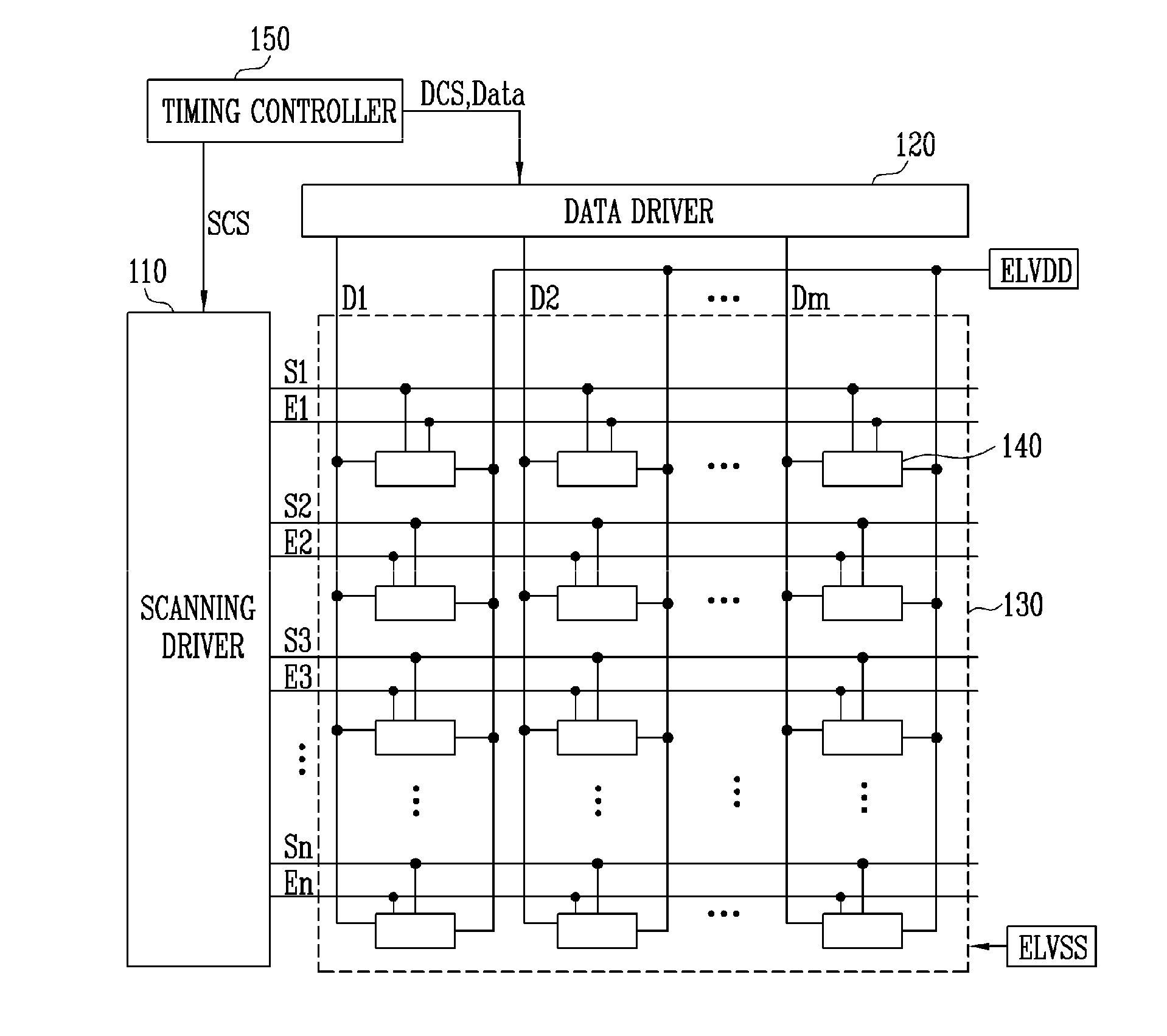
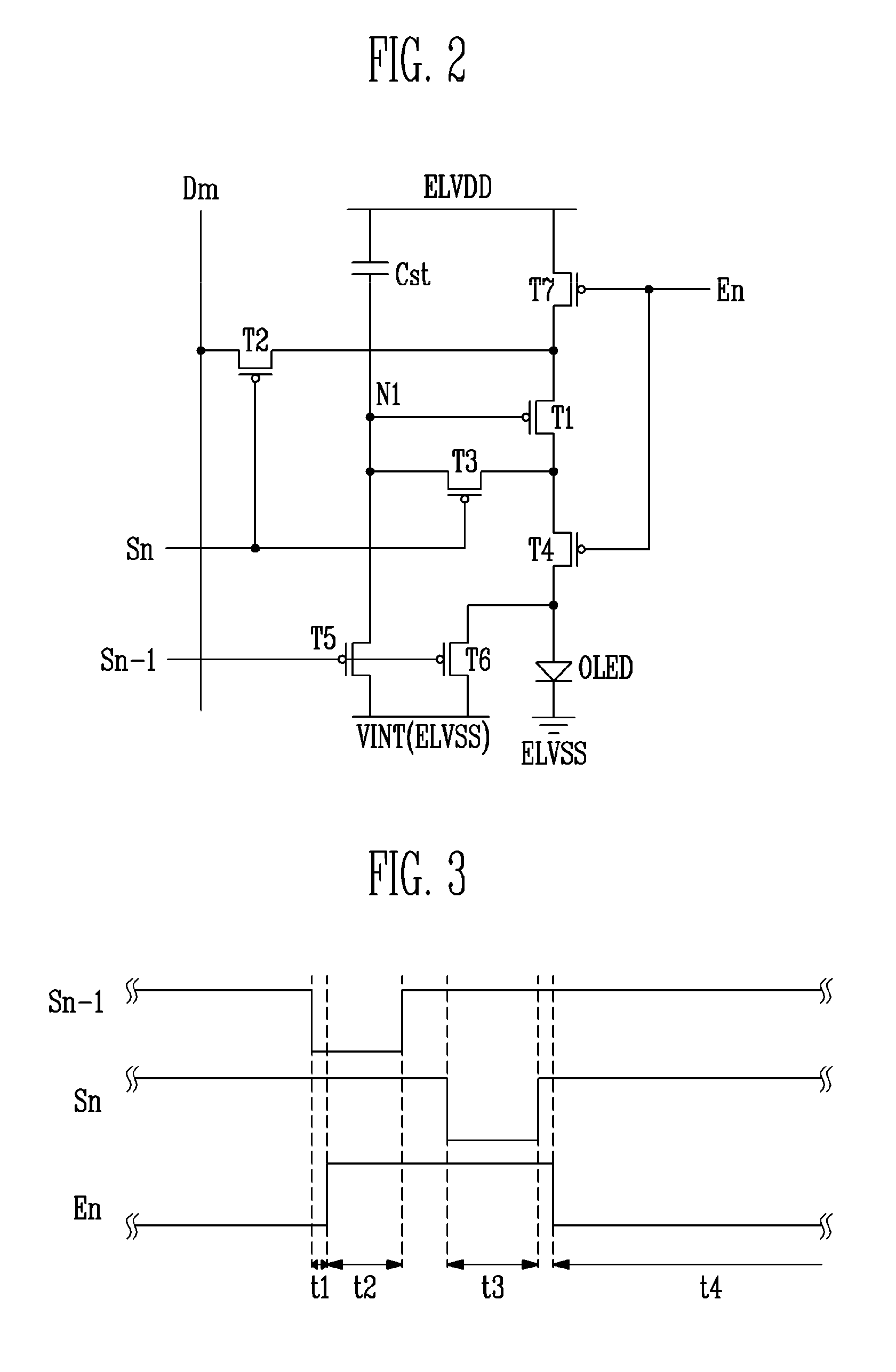
[0031]FIG. 1 is a block view showing an organic light emitting display device according to an embodiment of the present invention. Referring to FIG. 1, an organic light emitting display device according to an embodiment of the present invention includes a pixel unit 130 including a plurality of ...


PUM


Abstract

A pixel having an improved response time includes an organic light emitting diode connected between a first power supply and a second power supply; a first transistor connected between the first power supply and the organic light emitting diode, the first transistor including a gate electrode connected to a first node; a second transistor connected between a first electrode of the first transistor connected to the first power supply and a data line, the second transistor including a gate electrode connected to a current scanning line; a third transistor connected between a second electrode of the first transistor connected to the organic light emitting diode and the first node, the third transistor including a gate electrode connected to the current scanning line; a fourth transistor connected between the second electrode of the first transistor and the organic light emitting diode, the fourth transistor including a gate electrode connected to a light emitting control line; a fifth transistor connected between the second power supply or a third power supply that is an initialization power supply and the first node, the fifth transistor including a gate electrode connected to a previous scanning line; a sixth transistor connected between the second power supply or the third power supply and the fourth transistor, the sixth transistor including the gate electrode connected to the previous scanning line; and a storage capacitor connected between the first power supply and the first node.

Description

CROSS-REFERENCE TO RELATED APPLICATION[0001]This application claims priority to and the benefit of Korean Patent Application No. 10-2010-0062763, filed on Jun. 30, 2010, in the Korean Intellectual Property Office, the disclosure of which is incorporated herein by reference.BACKGROUND[0002]1. Field[0003]An aspect of the present invention relates to a pixel and an organic light emitting display device using the same, and more particularly, to an organic light emitting display device using a pixel that has an improved response time.[0004]2. Description of the Related Art[0005]Recently, all sorts of flat panel display devices are being developed, in which the flat panel display devices have a lighter weight and a smaller volume as compared to cathode ray tube devices.[0006]Especially, an organic light emitting display device, among the flat panel display devices, is being considered as the next generation display device because of its superior luminance and color purity. This is due to ...

Claims


Application Information

Patent Timeline
IPC IPC(8): G09G3/30G09G5/00H01L27/15
CPCG09G3/3233G09G2300/0819G09G2320/0261G09G2320/0238G09G2320/0252G09G2300/0861
Inventor JEONG, JIN-TAEKAWASHIMA, SHINGO
Owner SAMSUNG DISPLAY CO LTD
Why Eureka
Try Eureka