Controller apparatus for controlling a multiphase multilevel voltage source inverter and a method thereof
a multi-level voltage source and control apparatus technology, applied in control systems, power conversion systems, pulse duration/width modulation, etc., can solve problems such as expansion, reduced dc voltage usage rate thereof, and restricted use of several types of multi-phase svpwm
- Summary
- Abstract
- Description
- Claims
- Application Information
AI Technical Summary
Problems solved by technology
Method used
Image

Examples
first embodiment
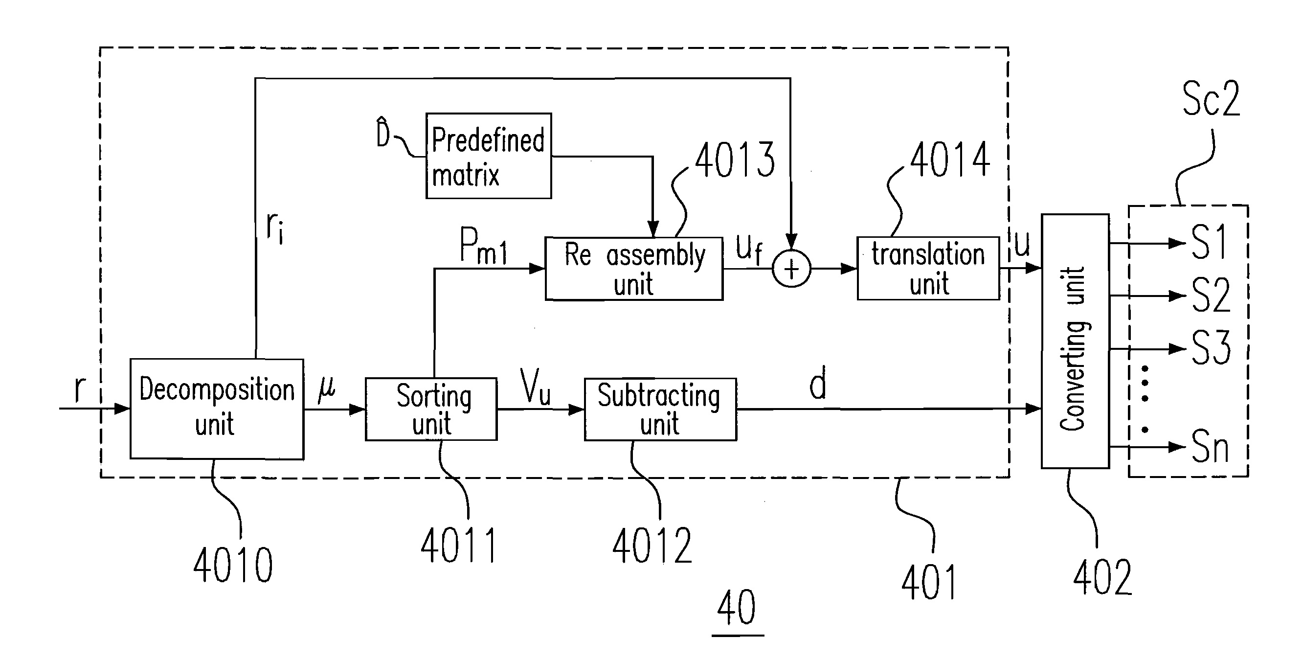
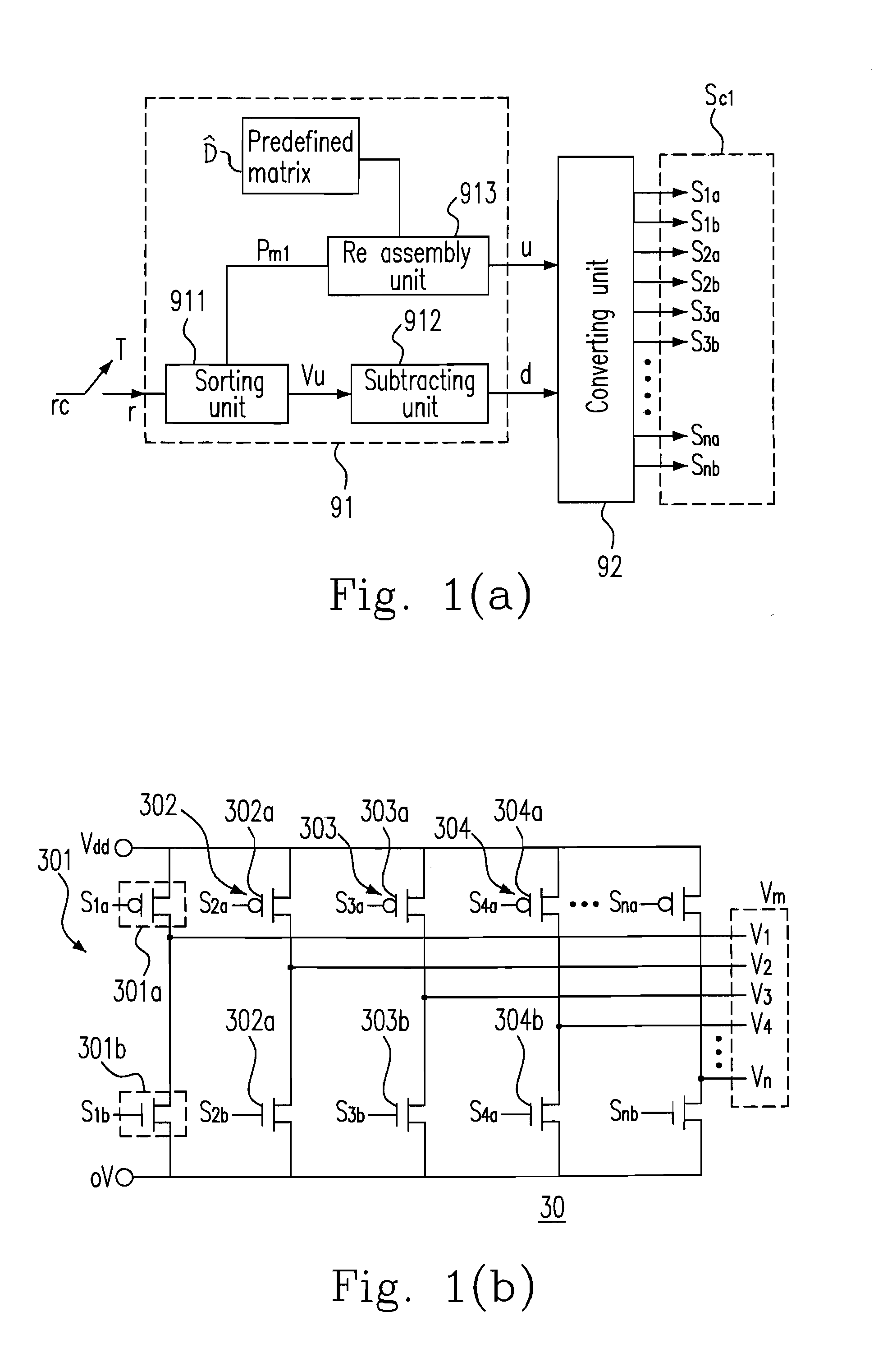
[0026]Please refer to FIG. 1(a), which is a schematic diagram showing an apparatus for controlling a two-level multiphase voltage source inverter in accordance with the present invention. The apparatus 9 for controlling a voltage source inverter includes a signal-generating unit 91 and a converting unit 92. The signal-generating unit 91 has a sorting unit 911, a subtracting unit 912 and a re-assembly unit 913.
[0027]The signal generating unit 91 responds to an input signal r to produce a switching strategy control signal u and a duration timing control signal d corresponding to the switching strategy control signal u. The converting unit 92 responds to the switching strategy control signal u and the duration timing control signal d to produce a switching signal Sc1. According to FIG. 1(a), the switching signal Sc1 includes S1a, S1b, S2a, S2b, . . . Sna and Snb.
[0028]Please refer to FIG. 1(b), which is a schematic diagram of a two-level multiphase voltage source inverter in accordance...
second embodiment
[0049]Please refer to FIGS. 3(a) to 3(c), which are the schematic diagrams of a 2-level voltage-switching unit, a 3-level voltage-switching unit and a multiple-level voltage-switching unit respectively, according to the present invention. In the illustrations of FIG. 3(a), the output voltage Vd can be either switched to DC voltage Vdc or zero. In FIG. 3(b), the output voltage Vd can be switched to DC voltage Vdc, a double DC voltage of Vdc or zero. In the illustrations of FIG. 3(c), the output voltage Vd can be switched to one selected from the group consisted of zero, DC voltage Vdc, a double DC voltage of Vdc, . . . , or a n−1 times of Vdc, where n is an integral.
[0050]Noted that the switching signal Sc2 in FIG. 2 includes switching signals S1, S2, S3 . . . and Sn. The switching signal Sc2 is generated based on the third matrix Pm3 and an input period of the duration time control signal d. The switching signal Sc2 can be used to control the voltage to be output from voltage switch...
PUM
 Abstract
Description
Claims
Application Information
 - R&D
- Intellectual Property
- Life Sciences
- Materials
- Tech Scout
- Unparalleled Data Quality
- Higher Quality Content
- 60% Fewer Hallucinations
Browse by: Latest US Patents, China's latest patents, Technical Efficacy Thesaurus, Application Domain, Technology Topic, Popular Technical Reports.
© 2025 PatSnap. All rights reserved.Legal|Privacy policy|Modern Slavery Act Transparency Statement|Sitemap|About US| Contact US: help@patsnap.com