

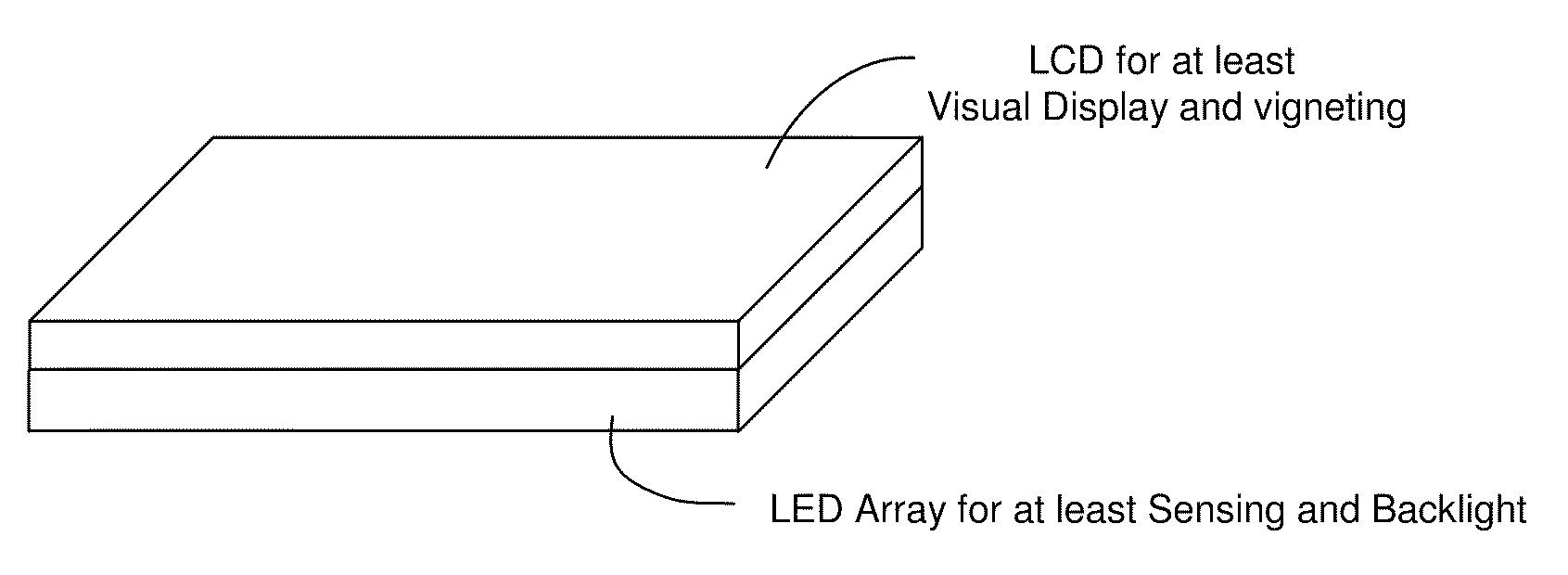
Led/oled array approach to integrated display, lensless-camera, and touch-screen user interface devices and associated processors
a technology of integrated display and array, which is applied in static indicating devices, instruments, material analysis, etc., can solve the problems of system hardware complexity, inter-chip communication complexity, and dramatic reduction of component count of contemporary and future mobile devices
- Summary
- Abstract
- Description
- Claims
- Application Information
AI Technical Summary
Benefits of technology
Problems solved by technology
Method used
Image

Examples
Embodiment Construction
[0086]The above and other aspects, features and advantages of the present invention will become more apparent upon consideration of the following description of preferred embodiments taken in conjunction with the accompanying drawing figures.
[0087]In the following description, reference is made to the accompanying drawing figures which form a part hereof, and which show by way of illustration specific embodiments of the invention. It is to be understood by those of ordinary skill in this technological field that other embodiments may be utilized, and structural, electrical, as well as procedural changes may be made without departing from the scope of the present invention.
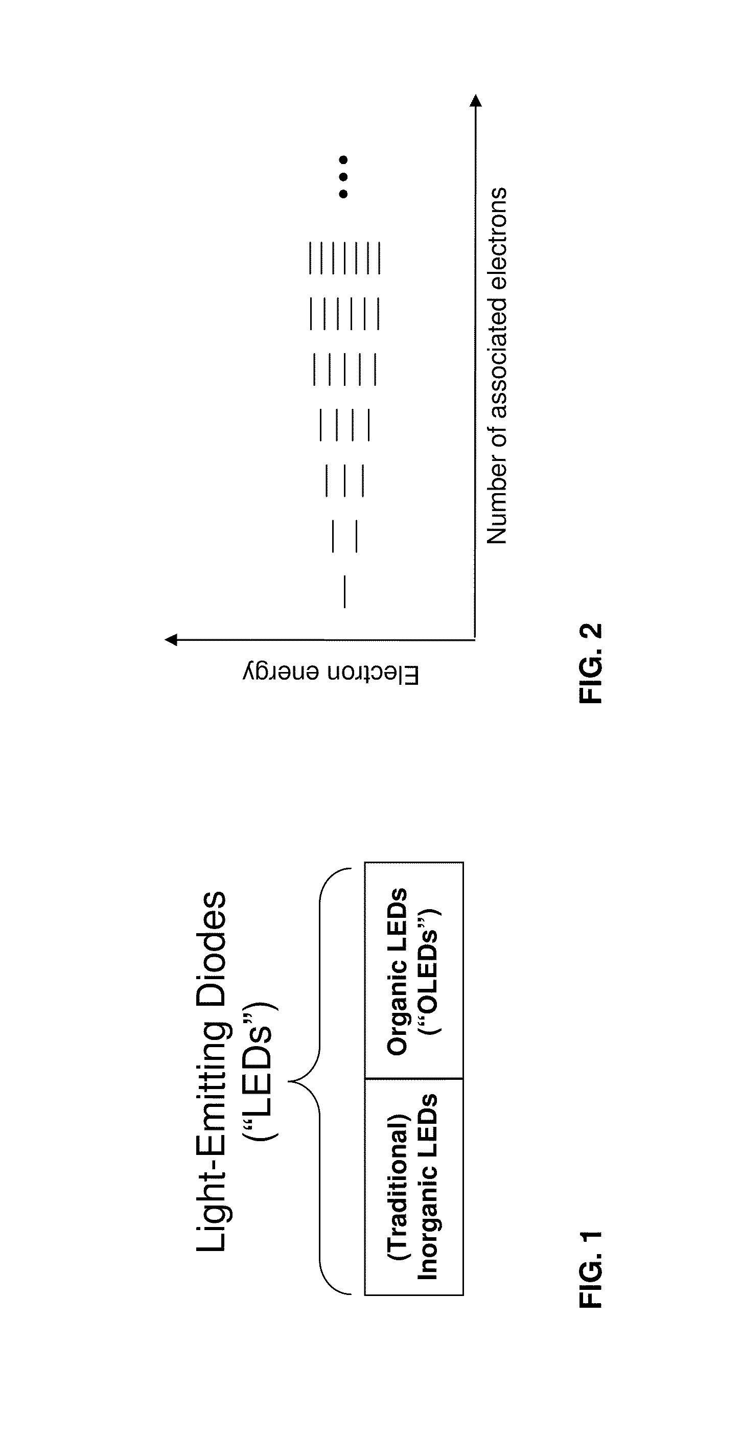
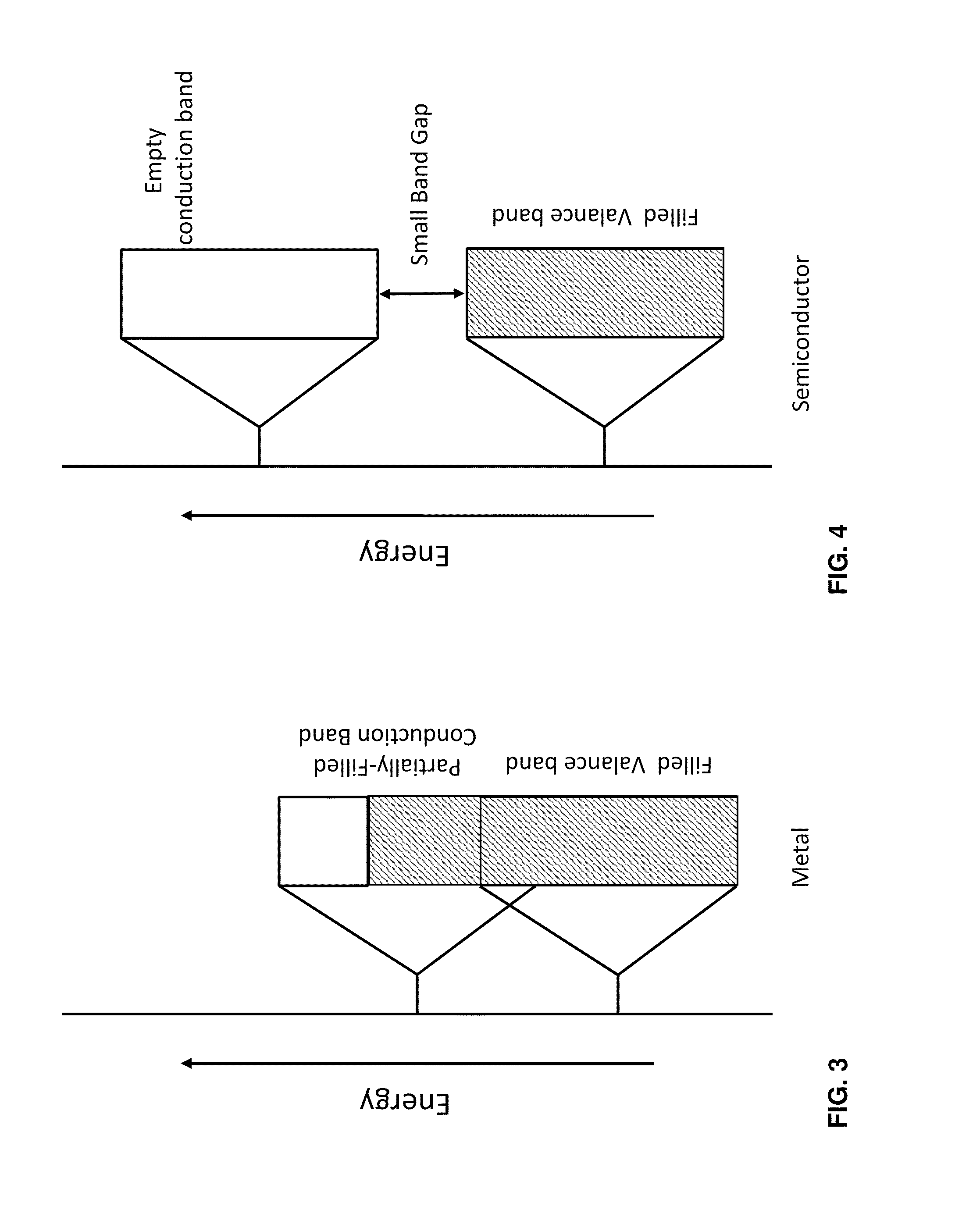
Inorganic and Organic Semiconductors
[0088]FIG. 2 depicts a representation of the spread of electron energy levels as a function of the number of associated electrons in a system such as a lattice of semiconducting material resultant from quantum state exclusion processes. As the number of associated electrons in a ...
PUM
 Abstract
Description
Claims
Application Information