Black silicon based metal-semiconductor-metal photodetector

a metal-semiconductor and metal-based technology, applied in the field of black silicon-based metal-semiconductor-metal photodetectors, can solve the problems of low sensitivity of silicon-based msm-pd, and achieve the effect of not complex design and manufacturing process

Active Publication Date: 2012-01-19
UNIV OF ELECTRONICS SCI & TECH OF CHINA
View PDF7 Cites 18 Cited by
  • Summary
  • Abstract
  • Description
  • Claims
  • Application Information

AI Technical Summary

Benefits of technology

[0007]An object of the present invention is to provide a black silicon based metal-semiconductor-metal photodetector, using the silicon as a basic material, which is compatible with the standard process, thus its design and manufacturing process is not complex.

Problems solved by technology

Therefore, the key issue to be resolved in the silicon-based MSM-PD is still the low sensitivity.

Method used


Image

  • Black silicon based metal-semiconductor-metal photodetector
  • Black silicon based metal-semiconductor-metal photodetector
  • Black silicon based metal-semiconductor-metal photodetector

Examples


Embodiment Construction

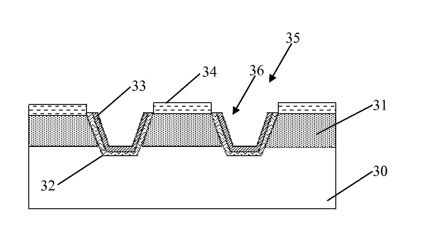
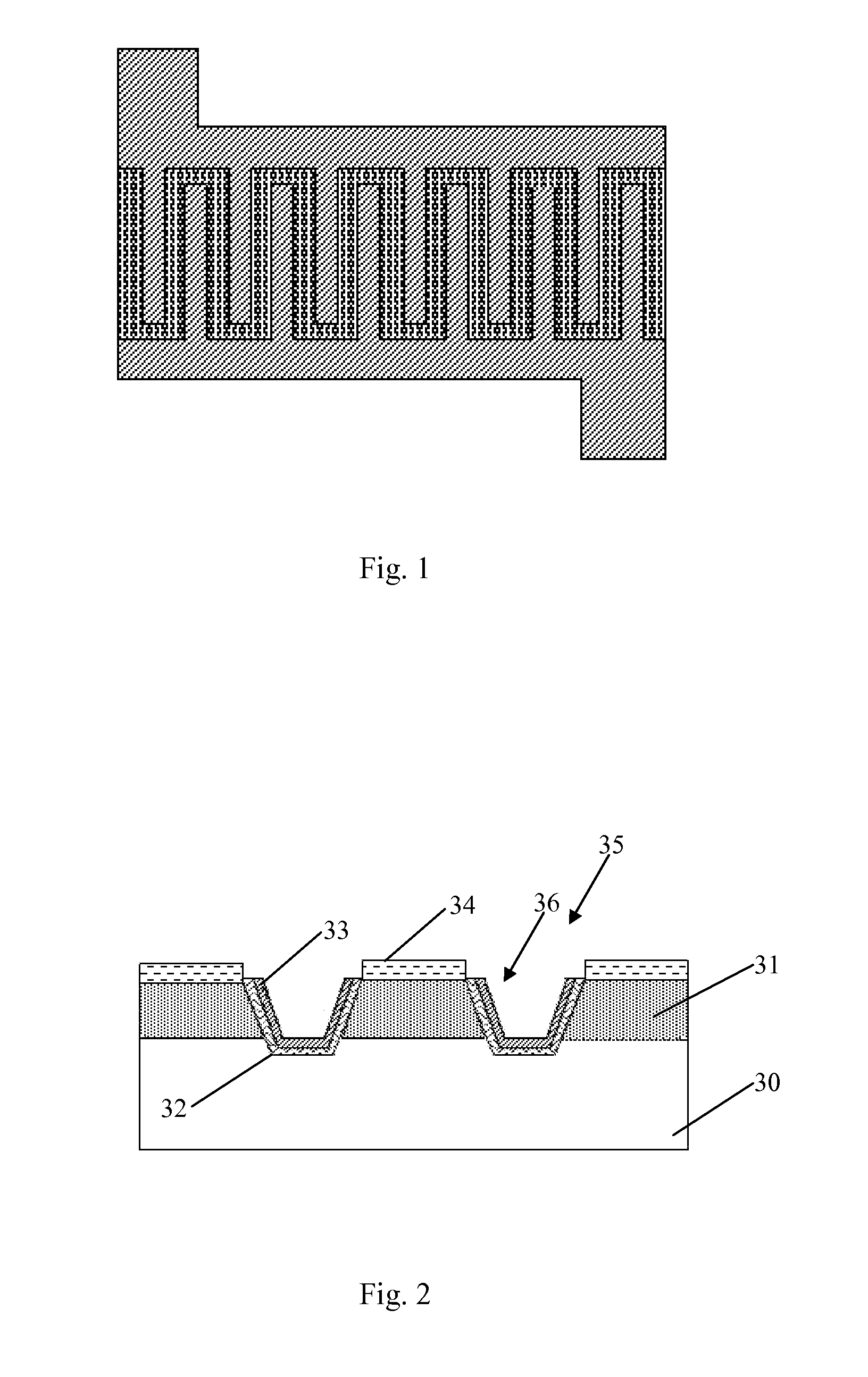
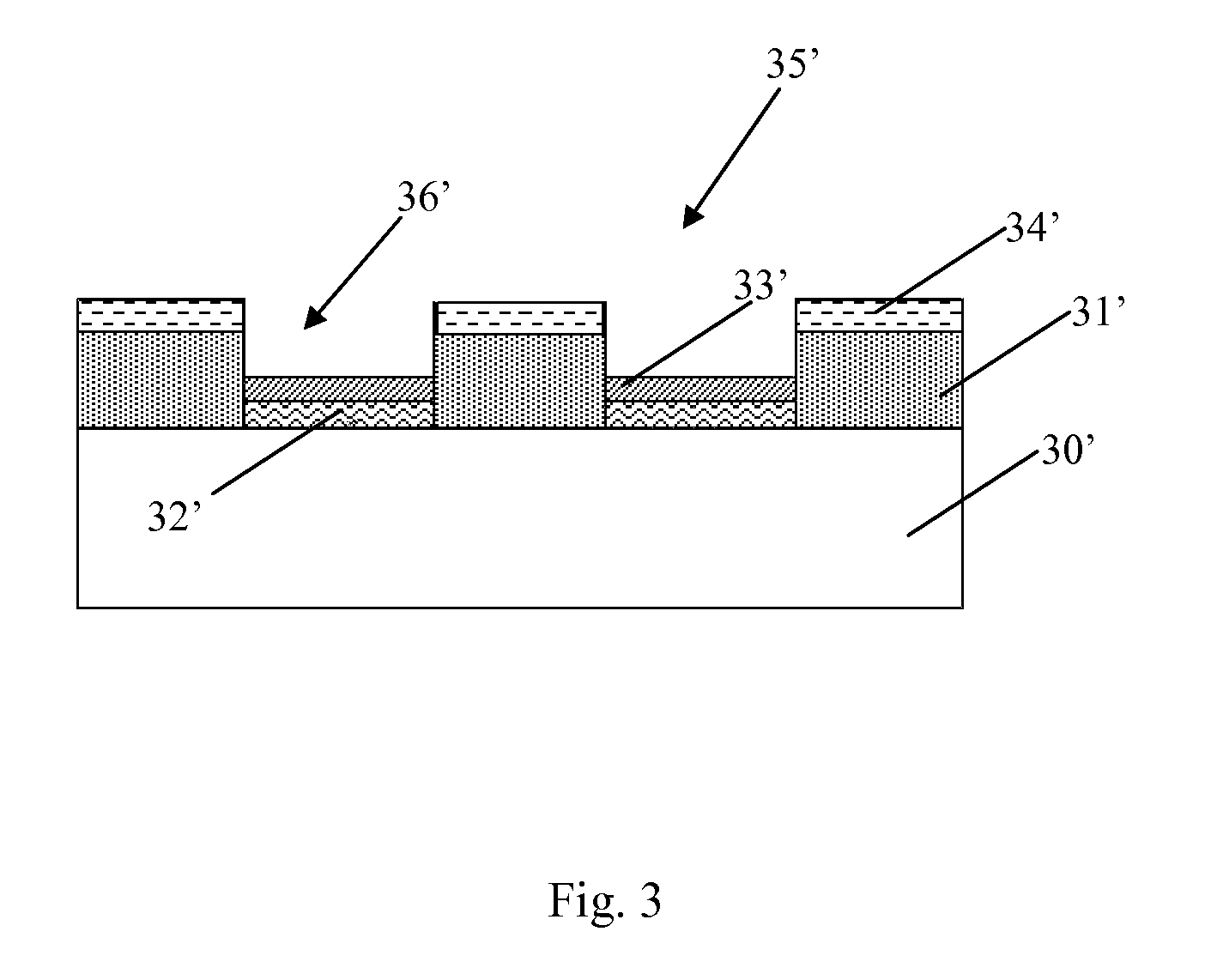
[0025]Black silicon is a silicon surface layer by a special treatment. Impurity elements with high concentration are introduced into a silicon substrate by an ion implantation for widening the spectrum absorption range of the silicon substrate. Furthermore, a microstructure anti-reflection layer is formed on a surface of the silicon substrate for reducing the light reflection to improve the light absorptivity. Therefore, the spectrum absorption range of the device based on black silicon will be widened, and the responsibility thereof will be improved.

[0026]A method of preparing a black silicon layer on a silicon substrate comprises the steps of:[0027](1) implanting a doping material by an ion implantation method into the silicon substrate;[0028](2) preparing a surface microstructure on a surface of the silicon substrate; and[0029](3) applying a vacuum heat treatment process to the doped silicon substrate with the surface microstructure.

[0030]In the step (1), the doping material can ...


PUM

PropertyMeasurementUnit
thicknessaaaaaaaaaa
thicknessaaaaaaaaaa
depthaaaaaaaaaa

Abstract

A black silicon based metal-semiconductor-metal photodetector includes a silicon substrate and a black silicon layer formed on the silicon substrate. An interdigitated electrode pattern structure is formed on the black silicon layer, which can be a planar or U-shaped structure. A thin potential barrier layer is deposited at the interdigitated electrode pattern structure. An Al or transparent conductive ITO thin film is deposited on the thin potential barrier layer. A passivation layer is provided on the black silicon layer. In the black silicon based metal-semiconductor-metal photodetector, the black silicon layer, as a light-sensitive area, can respond to ultraviolet, visible and near infrared light.

Description

BACKGROUND OF THE PRESENT INVENTION[0001]1. Field of Invention[0002]The present invention relates to a photoelectric detection technology, and more particularly to a black silicon based metal-semiconductor-metal photodetector and method of manufacture thereof.[0003]2. Description of Related Arts[0004]Silicon is an important semiconductor material, and currently also a main material used in the microelectronics integrated circuit process, and plays a very important role in the very large scale integrated circuit (VLSI). Compared with other compound optoelectronic devices, the optoelectronic devices and optoelectronic integrated circuits manufactured by the mature standard integrated circuit (IC) process using silicon as a basic material, will have a great advantage, however, the research on the silicon-based photodetector still has no great breakthrough at present. When the light wave is incident on the surface of the silicon-based optoelectronic device, the reflected light energy ca...

Claims


Application Information

Patent Timeline
Patent Type & Authority Applications(United States)
IPC IPC(8): H01L31/108H01L31/18
CPCH01L31/022425H01L31/022433H01L31/0236Y02E10/50H01L31/1085H01L31/202H01L31/035281H01L31/022408H01L31/02161H01L31/022475Y02P70/50
Inventor JIANG, YADONGZHAO, GUODONGWU, ZHIMINGLI, WEIJIANG, JINGZHANG, ANYUANGUO, ZHENGYU
Owner UNIV OF ELECTRONICS SCI & TECH OF CHINA
Why Eureka
Try Eureka