Asynchronous semiconductor memory capable of preventing coupling noise

a technology of asynchronous semiconductor memory and coupling noise, which is applied in the field of semiconductor memory, can solve the problems of memory not being equipped on the board, inaccurate data reading, and erroneous data reading, and achieve the effect of preventing coupling noise and accurately performing data reading

Active Publication Date: 2012-01-26
LAPIS SEMICON CO LTD
View PDF6 Cites 3 Cited by
  • Summary
  • Abstract
  • Description
  • Claims
  • Application Information

AI Technical Summary

Benefits of technology

[0009]Thus, a semiconductor memory according to the present invention is configured to, in driving (precharging) a bit line formed in a memory cell array when a certain delay period has elapsed after an address transition is detected, adjust the delay period based on an external setting through an input pad or an internal setting through a fuse device or cell fuse. As a result, in the case where the skew period of a supplied address is long, the delay period is extended, thereby preventing driving (precharging) from being carried out with respect to bit lines corresponding to unsettled addresses in the address skew period and allowing driving (precharging) to be carried out with respect to only a bit line corresponding to a next address after the lapse of the address skew period. Therefore, it is possible to prevent coupling noise resulting from sequential precharging with respect to bit lines corresponding to unsettled addresses and a bit line corresponding to a next address, so that data reading can be accurately performed.

Problems solved by technology

At this time, provided that one adjacent to the bit line corresponding to the “next address” is present among the respective bit lines corresponding to the group of unsettled addresses, coupling noise may accompany a cell recovery operation through the bit lines corresponding to the unsettled addresses, resulting in there being a concern that erroneous data reading could be carried out.
That is, provided that the address skew period allowed in the board is longer than the address skew period specified in the semiconductor memory, there may be a concern that erroneous data reading could be carried out, resulting in a problem that this semiconductor memory may not be equipped on the board.

Method used


Image

  • Asynchronous semiconductor memory capable of preventing coupling noise
  • Asynchronous semiconductor memory capable of preventing coupling noise
  • Asynchronous semiconductor memory capable of preventing coupling noise

Examples


Embodiment Construction

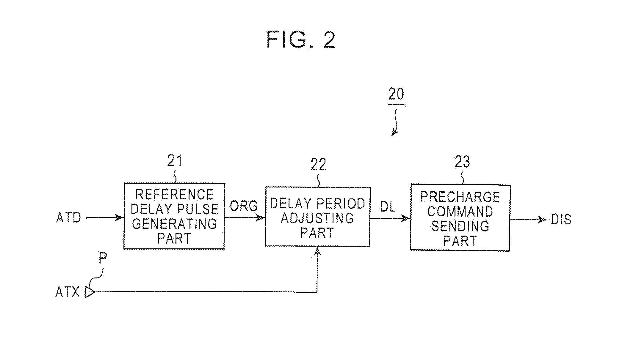
[0015]The present invention is configured to, in detecting whether an address transition has been made and precharging a bit line formed in a memory cell array when a certain delay period has elapsed after the address transition is detected, adjust the delay period based on a delay period extension signal.

[0016]Now, exemplary embodiments of the present invention will be described in detail with reference to the annexed drawings.

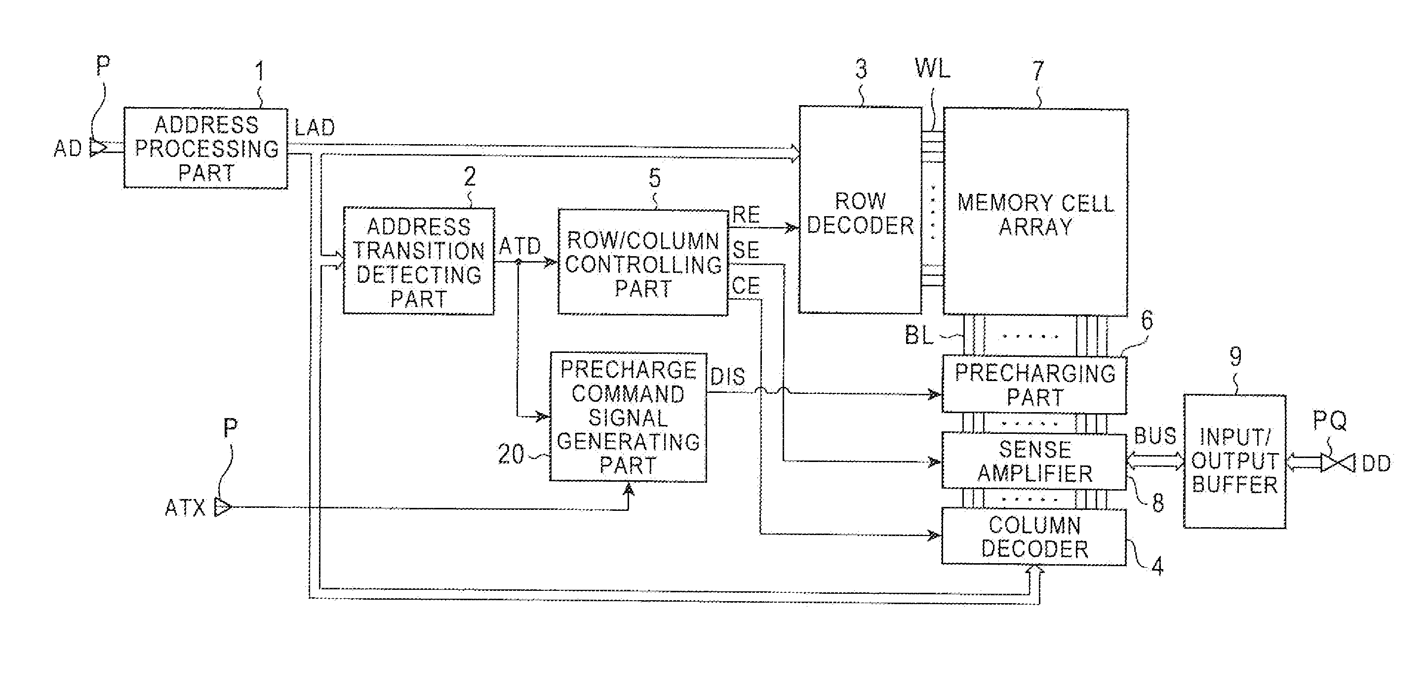
[0017]FIG. 1 is a block diagram showing a circuit configuration provided in a semiconductor memory according to the present invention.

[0018]In FIG. 1, an address processing part 1 receives n-bit (where n is an integer which is 2 or more) address data AD externally supplied through an input pad P of the semiconductor memory and supplies the received address data AD as internal address data LAD to an address transition detecting part 2, a row decoder 3 and a column decoder 4.

[0019]The address transition detecting part 2 detects whether a transition from an addr...


PUM


Abstract

Disclosed herein is a semiconductor memory which is capable of performing data reading without a faulty operation irrespective of the span of an address skew period. In detecting whether an address transition has been made and precharging a bit line formed in a memory cell array when a certain delay period has elapsed after the address transition is detected, the delay period is adjusted based on a delay period extension signal.

Description

BACKGROUND OF THE INVENTION[0001]1. Field of the Invention[0002]The present invention relates to a semiconductor memory, and more particularly to a semiconductor memory in which a bit line of a memory cell is precharged in a data read operation.[0003]2. Description of the Related Art[0004]An asynchronous semiconductor memory has been known in which a bit line of a memory cell begins to be precharged when a transition to a next address is detected, and data is read after the precharging is completed (see FIG. 1 of Japanese Patent Kokai No. 2003-85970 (Patent Literature 1) as an example). In this semiconductor memory, an address transition detection (ATD) circuit detects whether a transition to a next address has been made, and generates an address change detection signal ATD as a result of the detection. A precharge enable signal PE is generated based on the address change detection signal ATD, and precharging is performed with respect to a bit line of a memory cell corresponding to ...

Claims


Application Information

Patent Timeline
Patent Type & Authority Applications(United States)
IPC IPC(8): G11C8/08
CPCG11C8/08
Inventor KURAMORI, BUNSHO
Owner LAPIS SEMICON CO LTD
Why Eureka
Try Eureka