LED package and method for manufacturing the same

Inactive Publication Date: 2012-02-02
ADVANCED OPTOELECTRONICS TECH
View PDF4 Cites 31 Cited by
  • Summary
  • Abstract
  • Description
  • Claims
  • Application Information

AI Technical Summary

Problems solved by technology

The use of a mold increases the cost of manufacturing the LED package.
The waiting of time for the melted encapsulation to be cooled is time-consuming, which decreases the

Method used


Image

  • LED package and method for manufacturing the same
  • LED package and method for manufacturing the same
  • LED package and method for manufacturing the same

Examples


Example

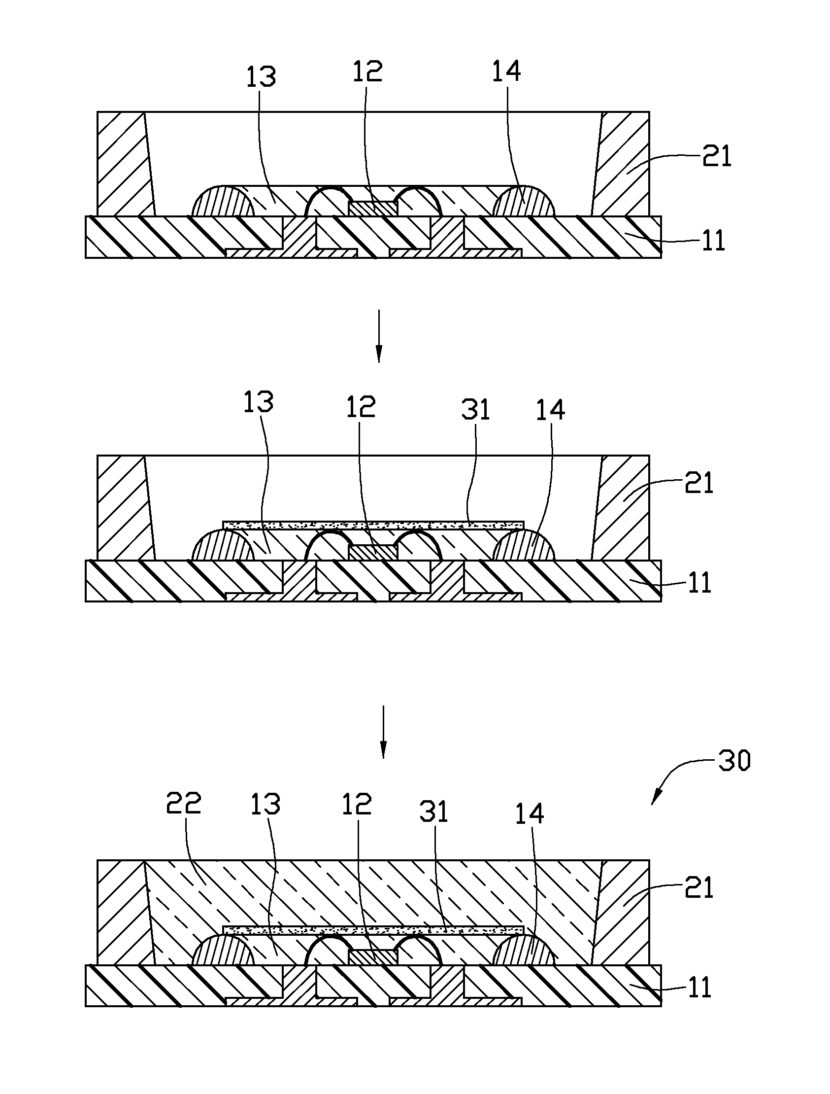
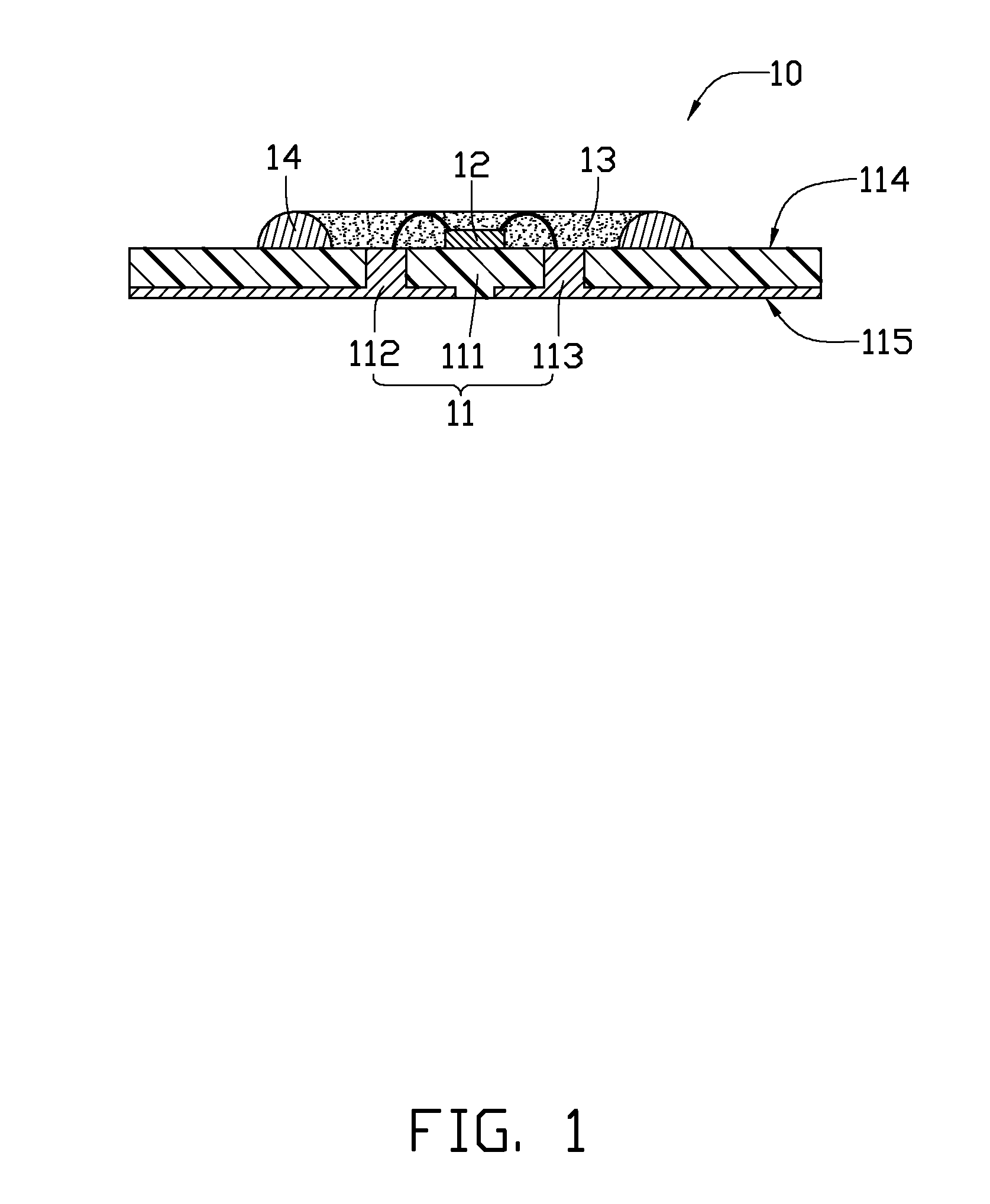
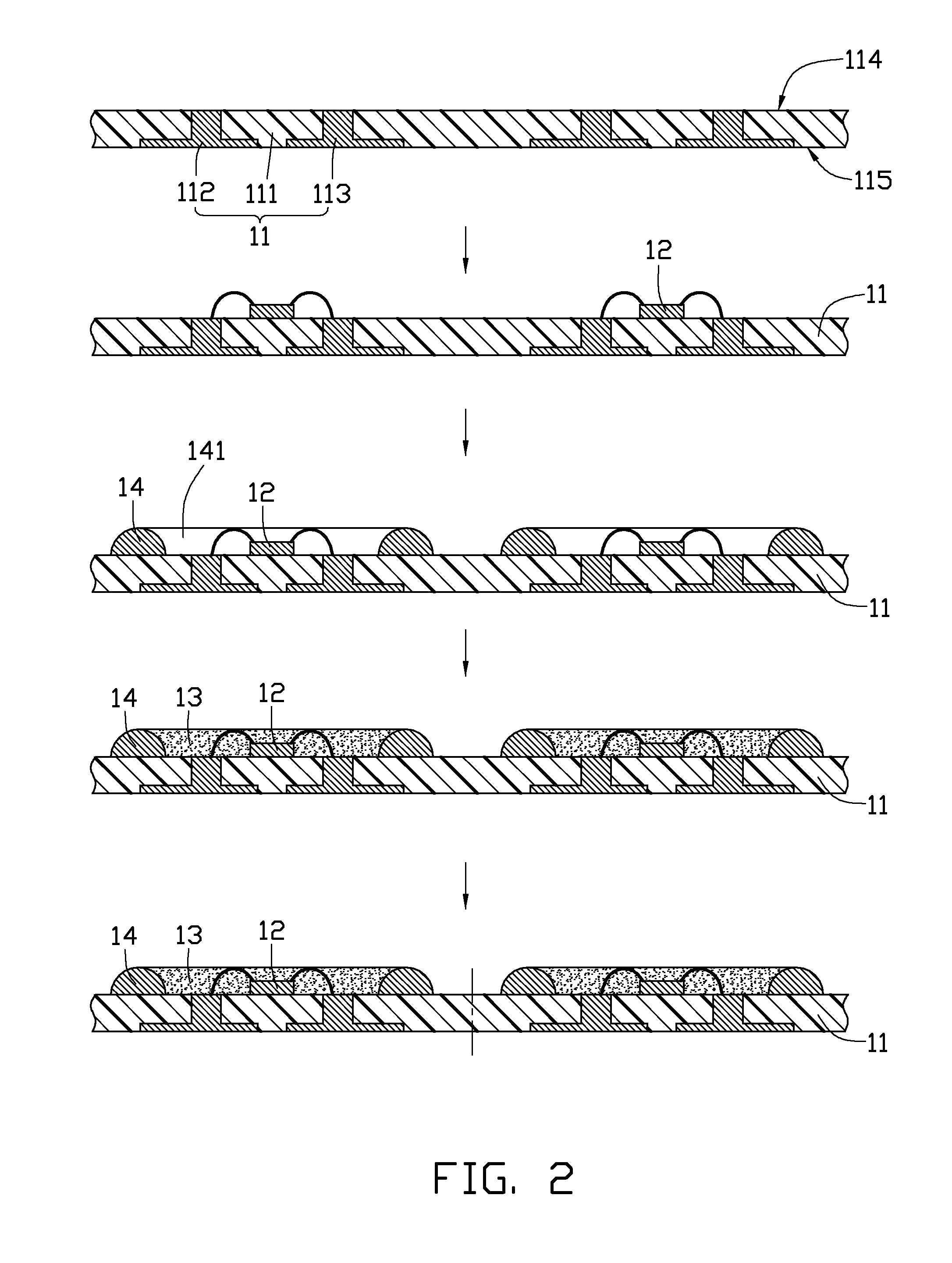
[0013]Embodiments of the present disclosure will now be described in detail below, with reference to the accompanying drawing.

[0014]Referring to FIG. 1, an LED package 10 according to a first exemplary embodiment is shown. The LED package 10 includes a substrate 11, an LED chip 12, a first encapsulation 13, and a bounding dam 14.

[0015]The substrate 11 includes an insulator 111, a first electrode 112 and a second electrode 113. The insulator 111 includes a first surface 114 and a second surface 115 opposite to the first surface 114. Each of the first electrode 112 and the second electrode 113 extends from the first surface 114 to the second surface 115, so that the LED package 10 can be conveniently mounted on a circuit board (not shown) using surface mounting technology. The insulator 111 is made of thermally conductive and electrically insulating material such as epoxy, silicone, silicon oxide or a mixture thereof. The first electrode 112 and the second electrode 113 can be made of...


PUM


Abstract

An LED package includes a substrate, an LED chip, a bounding dam, and a first encapsulation. The substrate includes a first surface and a second surface opposite to the first surface. The LED chip is mounted on the first surface of the substrate. The bounding dam is formed on the first surface of the substrate and surrounds the LED chip. The bounding dam and the substrate cooperatively define a receiving space. The bounding dam is made of thermoset resin. The first encapsulation is formed in the receiving space and encloses the LED chip.

Description

BACKGROUND[0001]1. Technical Field[0002]The present disclosure relates to semiconductor packages and, particularly, to an LED (light emitting diode) package and a method for manufacturing the LED package.[0003]2. Description of Related Art[0004]Typically, an LED package includes a substrate, an LED chip mounted on the substrate, and an encapsulation formed on the substrate to enclose the LED chip. The encapsulation is usually formed on the substrate by molding; that is, the encapsulation is formed by filling melted encapsulation into a mold and then being solidified after cooling. Thereafter, the mold is removed to leave the solidified encapsulation. The use of a mold increases the cost of manufacturing the LED package. The waiting of time for the melted encapsulation to be cooled is time-consuming, which decreases the manufacturing efficiency of the LED package. Finally, the removal of the mold may cause a damage to the solidified encapsulation if the operation is not carefully pro...

Claims


Application Information

Patent Timeline
IPC IPC(8): H01L33/46
CPCH01L33/486H01L33/54H01L33/60H01L2933/005H01L2224/48235H01L2224/48091H01L2224/48227H01L2924/12041H01L2924/01322H01L24/97H01L2924/00014H01L2924/00
Inventor LIN, SHEN-BO
Owner ADVANCED OPTOELECTRONICS TECH
Why Eureka
Try Eureka