Method of fabricating a multilayer structure with circuit layer transfer

Inactive Publication Date: 2012-02-02
SONY SEMICON SOLUTIONS CORP
View PDF6 Cites 10 Cited by
  • Summary
  • Abstract
  • Description
  • Claims
  • Application Information

AI Technical Summary

Benefits of technology

[0014]The aim of the invention is to propose a solution that, during fabrication of multilayer or composite structures, can reduce the phenomenon of overlay and distortion between the microcomponents formed on one face of a first substrate and the microcomponents subsequently formed on another face of the substrate after transfer onto a second substrate.
[0016]Thus, by holding, during bonding, one of the two substrates flush against a support of holding surface, i.e., the surface with which the substrate is held flush, that presents at its surface a flatness that is identical to or less than that of the holding surface of the support used during formation of the microcomponents, the risks of overlay and distortion during subsequent formation of additional layers of microcomponents are substantially reduced.
[0017]By fixing the first substrate during bonding in a geometric configuration, at least in terms of bow / warp type deformations, that is similar to that presented thereby when the microcomponents are formed, it is possible to regain that geometric configuration during formation of an additional layer of microcomponents on the other face of the first substrate. Even if the first substrate has a different geometry once released following bonding, for example. due to the difference in geometry compared with the second substrate, the first substrate regains its geometry presented at the moment of bonding when the second substrate was being held flush against a support having a similar flatness to that of the flat reference support used during production of the microcomponents. In this manner, during formation of the second layer of microcomponents on the face of the first substrate opposite to that comprising the first layer of microcomponents or on the exposed face of the first layer, the reliability of the alignment of the photolithography mask with the microcomponents of the first layer or the first face of the layer and, as a result, the quality and value of the wafer are improved.

Problems solved by technology

However, the applicants have discerned that following transfer, there are circumstances where it is very difficult, if not impossible, to form additional microcomponents that are aligned with all of the microcomponents formed before the transfer.
As a consequence, this results in a phenomenon of misalignment (also known as overlay) between the two layers of microcomponents 11 and 12 that may be the source of short circuits or connection faults between the microcomponents of the two layers.
That phenomenon of overlay thus results in a reduction in the quality and value of the multilayer semiconductor wafers that are fabricated.
However, it has been observed that this misalignment is not homogeneous (i.e., cannot be reduced to elementary transformations); thus, it is not possible to correct the photolithography exposure in a general and satisfactory manner in order to obtain, for each exposed field of the wafer, a satisfactory maximum value for the overlay (for example, less than 100 nm [nanometer] or 50 nm).
Under such circumstances, it is not possible to compensate for overlays existing between the microcomponents of the two layers by lithography.

Method used


Image

  • Method of fabricating a multilayer structure with circuit layer transfer
  • Method of fabricating a multilayer structure with circuit layer transfer
  • Method of fabricating a multilayer structure with circuit layer transfer

Examples


Embodiment Construction

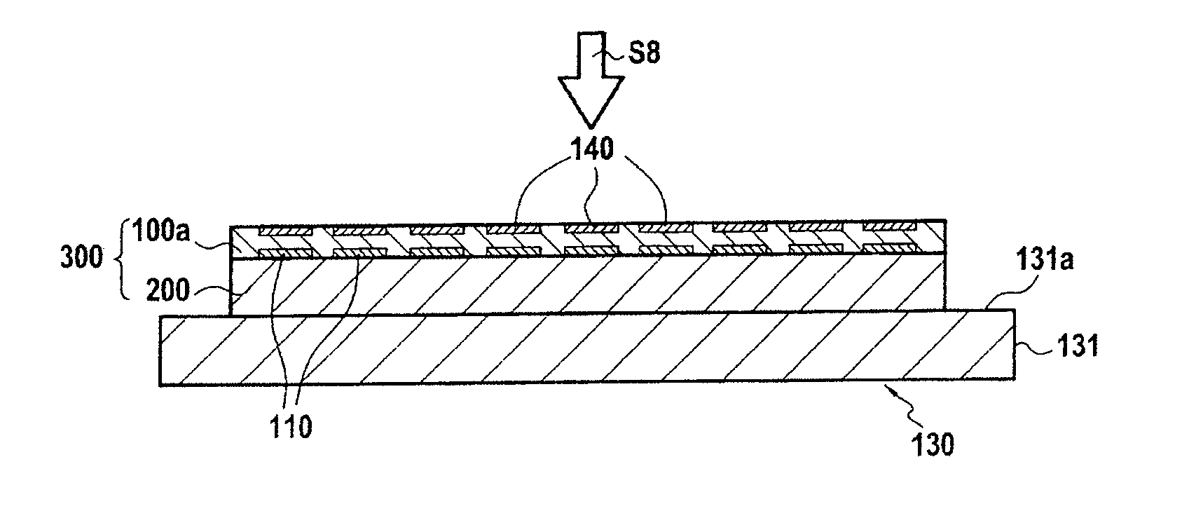
[0035]The present invention is of general application to the production of composite structures comprising at least bonding, for example, by wafer bonding, a first substrate or wafer comprising components onto a second substrate or wafer.

[0036]As described above, after bonding, the geometry of the first substrate is different from that which it had when the components thereof were being formed. As a consequence, after bonding, offsets are created in the structures of the first substrate, which causes an overlay and a distortion between the originally formed components and those formed subsequently.

[0037]In order to minimize these phenomena and to allow the subsequent production of components in alignment with those formed on the first substrate before bonding, the present invention proposes holding, during bonding, one of the two substrates on a support of holding surface that has a flatness similar to or less than that of the support used to hold the first substrate during formatio...


PUM


Abstract

A method of producing a composite structure comprises a step of producing a first layer of microcomponents on one face of a first substrate, the first substrate being held flush against a holding surface of a first support during production of the microcomponents, and a step of bonding the face of the first substrate comprising the layer of microcomponents onto a second substrate. During the bonding step, the first substrate is held flush against a second support, the holding surface of which has a flatness that is less than or equal to that of the first support used during production of the first layer of microcomponents.

Description

CROSS-REFERENCE TO RELATED APPLICATIONS[0001]This is a national phase entry under 35 U.S.C. §371 of International Patent Application PCT / EP2010 / 052765, filed Mar. 4, 2010, published in English as International Patent Publication WO 2010 / 102943 A1 on Sep. 16, 2010, which claims the benefit under Article 8 of the Patent Cooperation Treaty to French Patent Application Serial No. 0951543, filed Mar. 12, 2009, the entire disclosure of each of which is hereby incorporated herein by this reference.TECHNICAL FIELD[0002]The present invention relates to the field of multilayer semiconductor structures (also known as multilayer semiconductor wafers) produced by transferring at least one layer formed from an initial substrate onto a final substrate, the layer corresponding to the portion of initial substrate in which a plurality of microcomponents has been formed, for example.BACKGROUND[0003]Three-dimensional component integration technology (3D-integration) requires the transfer of one or more...

Claims


Application Information

Patent Timeline
IPC IPC(8): H01L21/762B65D85/00
CPCH01L21/2007H01L21/20H01L21/762
Inventor CASTEX, ARNAUDBROEKAART, MARCEL
Owner SONY SEMICON SOLUTIONS CORP
Why Eureka
Try Eureka