Flip chip package utilizing trace bump trace interconnection

a chip and trace technology, applied in the field of flip chip packaging, can solve the problems of limiting process window, reliability and throughput, and reducing the cost of substrate, so as to widen the process window for flip chip assembly

Active Publication Date: 2012-02-09
MEDIATEK INC
View PDF3 Cites 44 Cited by
  • Summary
  • Abstract
  • Description
  • Claims
  • Application Information

AI Technical Summary

Benefits of technology

[0010]It is one object of the invention to provide an improved flip chip package utilizing novel trace bump trace (TBT) interconnection, which is capable of lowering the cost in substrate and widening the process window for flip chip assembly flow.

Problems solved by technology

One drawback of the above-described prior art is that there is considerable loss of routing space on the top layer of package substrate 2.
Another drawback of the above-described prior art is that the small stand-off height between the die and the package substrate limits the process window, reliability and throughput when performing underfill process in the flip chip assembly flow.

Method used


Image

  • Flip chip package utilizing trace bump trace interconnection
  • Flip chip package utilizing trace bump trace interconnection
  • Flip chip package utilizing trace bump trace interconnection

Examples


Embodiment Construction

[0023]In the following detailed description of the invention, reference is made to the accompanying drawings which form a part hereof, and in which is shown, by way of illustration, specific embodiments in which the invention may be practiced. These embodiments are described in sufficient detail to enable those skilled in the art to practice the invention. Other embodiments may be utilized and structural, logical, and electrical changes may be made without departing from the scope of the present invention.

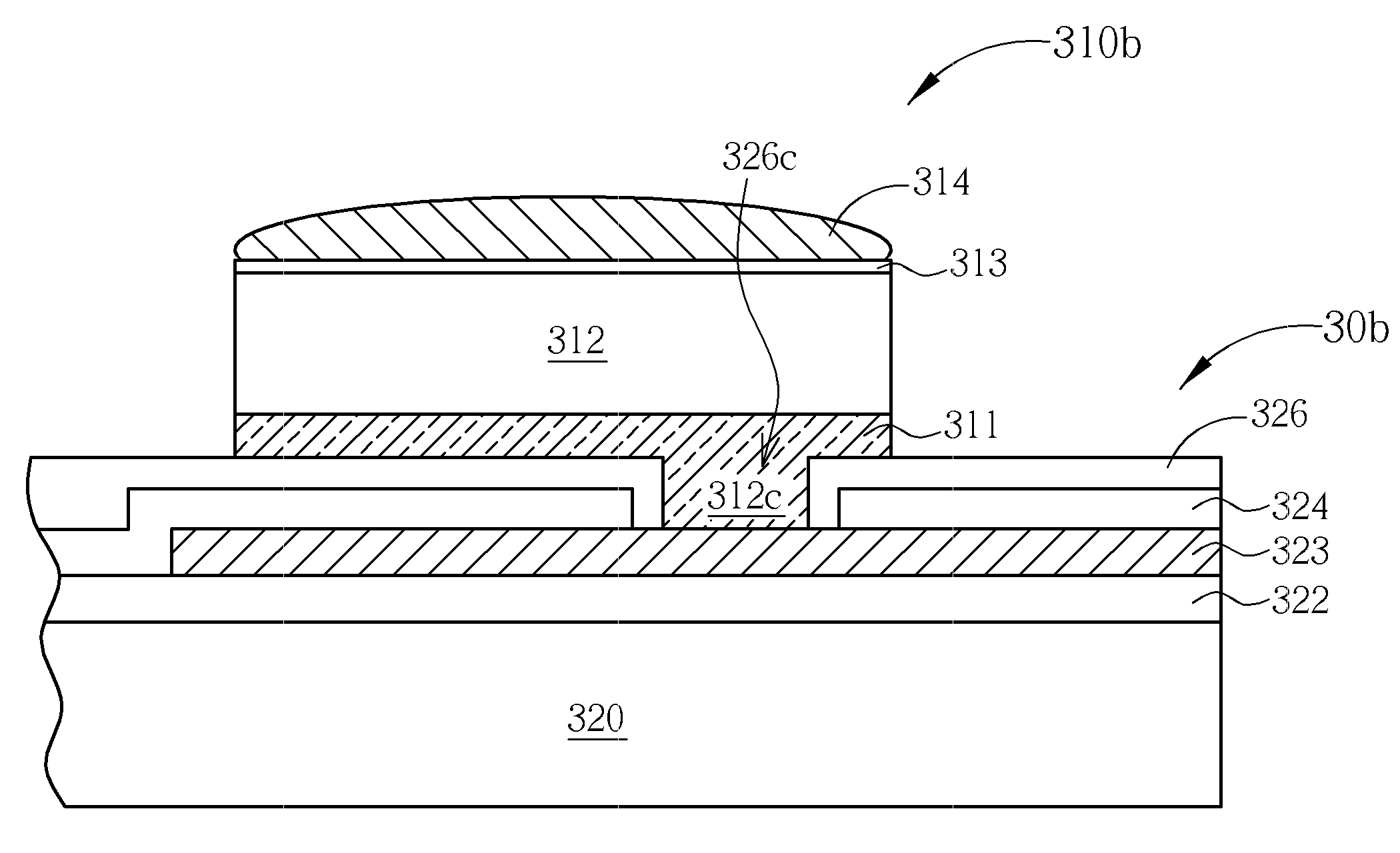
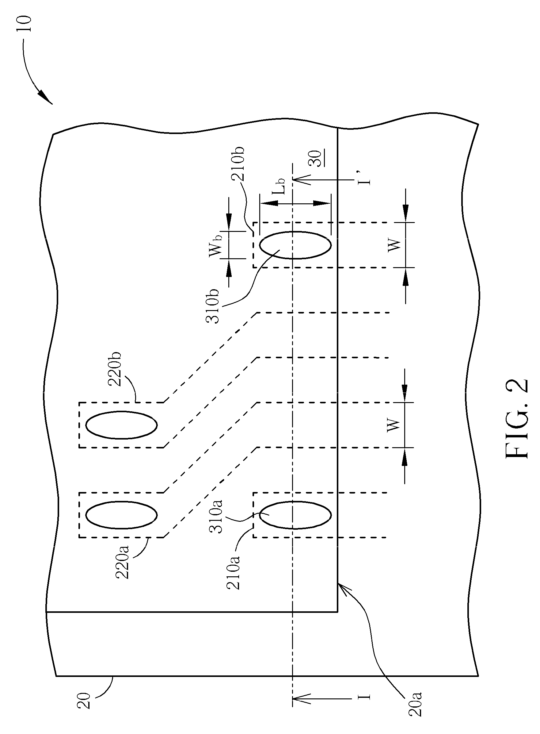
[0024]Please refer to FIG. 2 and FIG. 3. FIG. 2 is a plan view showing a portion of a flip chip package in accordance with one embodiment of this invention. FIG. 3 is a partial sectional view taken along line I-I′ in FIG. 2. As shown in FIG. 2 and FIG. 3, the flip chip package 10 comprises a package substrate 20 having a die attach surface 20a. A plurality of traces 210a, 210b, 220a and 220b, which are indicated by dotted lines in FIG. 2, are disposed on the die attach surface 20a ...


PUM


Abstract

A flip chip package includes a substrate having a die attach surface; and a die mounted on the die attach surface with an active surface of the die facing the substrate, wherein the die is interconnected to the substrate via a plurality of copper pillar bumps on the active surface, wherein at least one of the plurality of copper pillar bumps has a bump width that is substantially equal to or smaller than a line width of a trace on the die attach surface of the substrate.

Description

CROSS REFERENCE TO RELATED APPLICATIONS[0001]This application claims the benefit of U.S. provisional application No. 61 / 371,291 filed Aug. 6, 2010.BACKGROUND OF THE INVENTION[0002]1. Field of the Invention[0003]The present invention relates generally to flip chip technology. More particularly, the present invention relates to a flip chip package utilizing trace bump trace (TBT) interconnection.[0004]2. Description of the Prior Art[0005]In order to ensure miniaturization and multi-functionality of electronic products or communication devices, semiconductor packages are required to be of small in size, multi-pin connection, high speed, and high functionality. Increased Input-Output (I / O) pin count combined with increased demands for high performance ICs has led to the development of flip chip packages.[0006]Flip-chip technology uses bumps on chip to interconnect the package media such as package substrate. The flip-chip is bonded face down to the package substrate through the shortest...

Claims


Application Information

Patent Timeline
Patent Type & Authority Applications(United States)
IPC IPC(8): H01L23/498
CPCH01L21/563H01L2224/0401H01L23/49838H01L24/05H01L24/13H01L24/16H01L24/81H01L2224/0345H01L2224/05011H01L2224/0519H01L2224/05559H01L2224/05647H01L2224/05666H01L2224/13014H01L2224/13082H01L2224/13083H01L2224/13147H01L2224/13155H01L2224/16238H01L2224/81815H01L2924/01013H01L2924/01029H01L2924/01082H01L2924/014H01L2924/3511H01L23/3192H01L24/17H01L2224/73204H01L2224/32225H01L2224/16225H01L2924/01075H01L2924/01074H01L2924/01033H01L2924/01019H01L2924/00014H01L2224/131H01L2924/00H01L2924/00012H01L2924/14H01L2224/1308H01L2224/05569H01L2224/05008
Inventor LIN, TZU-HUNGGREGORICH, THOMAS MATTHEW
Owner MEDIATEK INC
Why Eureka
Try Eureka