Apparatus and method for temperature control during polishing

a technology of temperature control and polishing surface, which is applied in the direction of grinding drives, manufacturing tools, lapping machines, etc., can solve the problems of non-planar artifacts on the substrate surface, and achieve the effect of improving the polishing uniformity

Inactive Publication Date: 2012-02-16
APPLIED MATERIALS INC
View PDF4 Cites 23 Cited by
  • Summary
  • Abstract
  • Description
  • Claims
  • Application Information

AI Technical Summary

Benefits of technology

[0009]The present invention generally relates to a method and apparatus for polishing semiconductor substrates. Particularly, embodiments of the present invention provide apparatus and method for improving polishing uniformity.

Problems solved by technology

However, various factors of CMP process can lead to non-uniformity causing non-planar artifacts on the substrate surface.
Consequently, temperature variations within the substrate may lead to non-uniformity, such as non-planar surface, within the substrate.
For example, FIG. 1 illustrates a prior art polishing result with non-uniformity.

Method used


Image

  • Apparatus and method for temperature control during polishing
  • Apparatus and method for temperature control during polishing
  • Apparatus and method for temperature control during polishing

Examples


Embodiment Construction

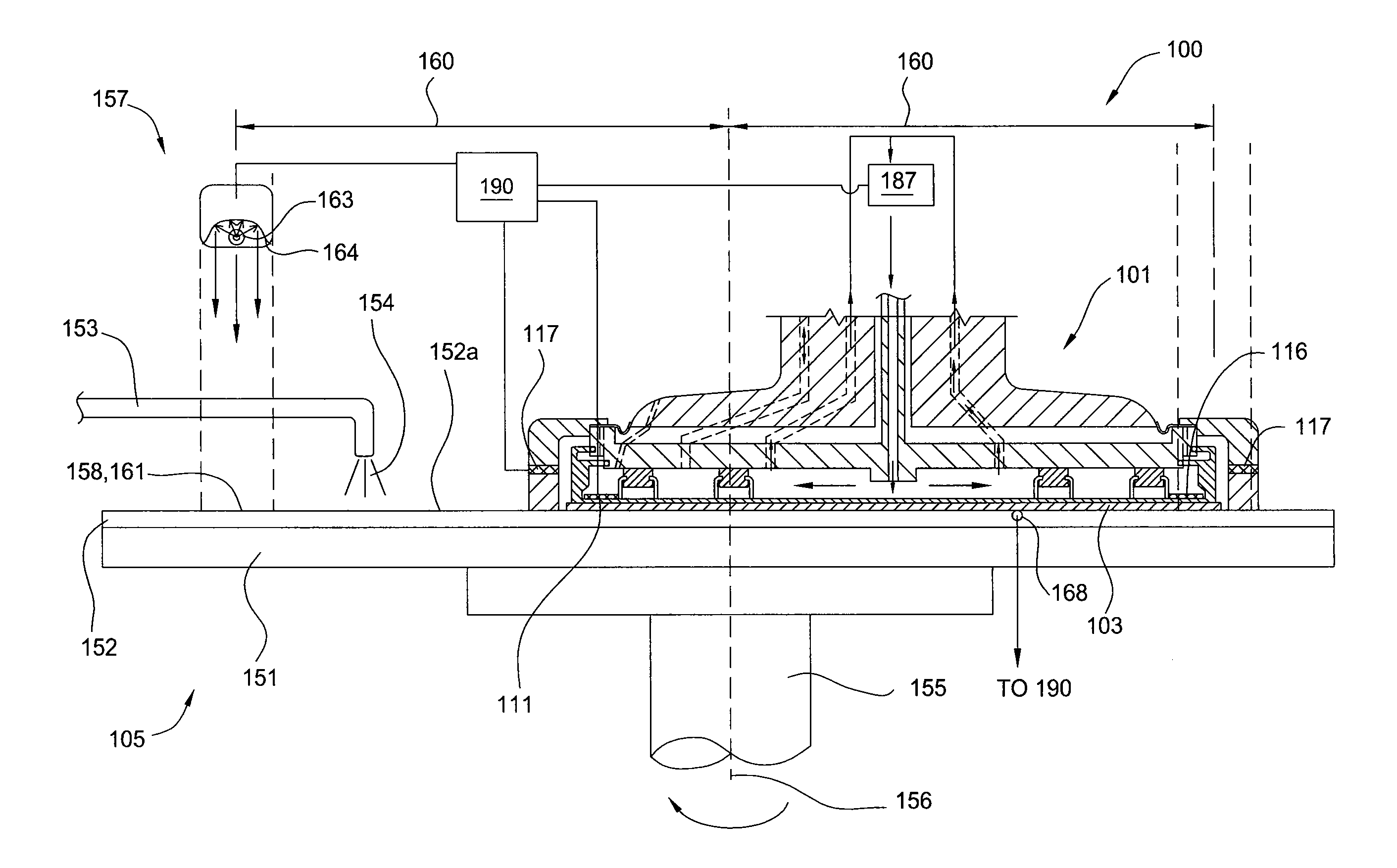
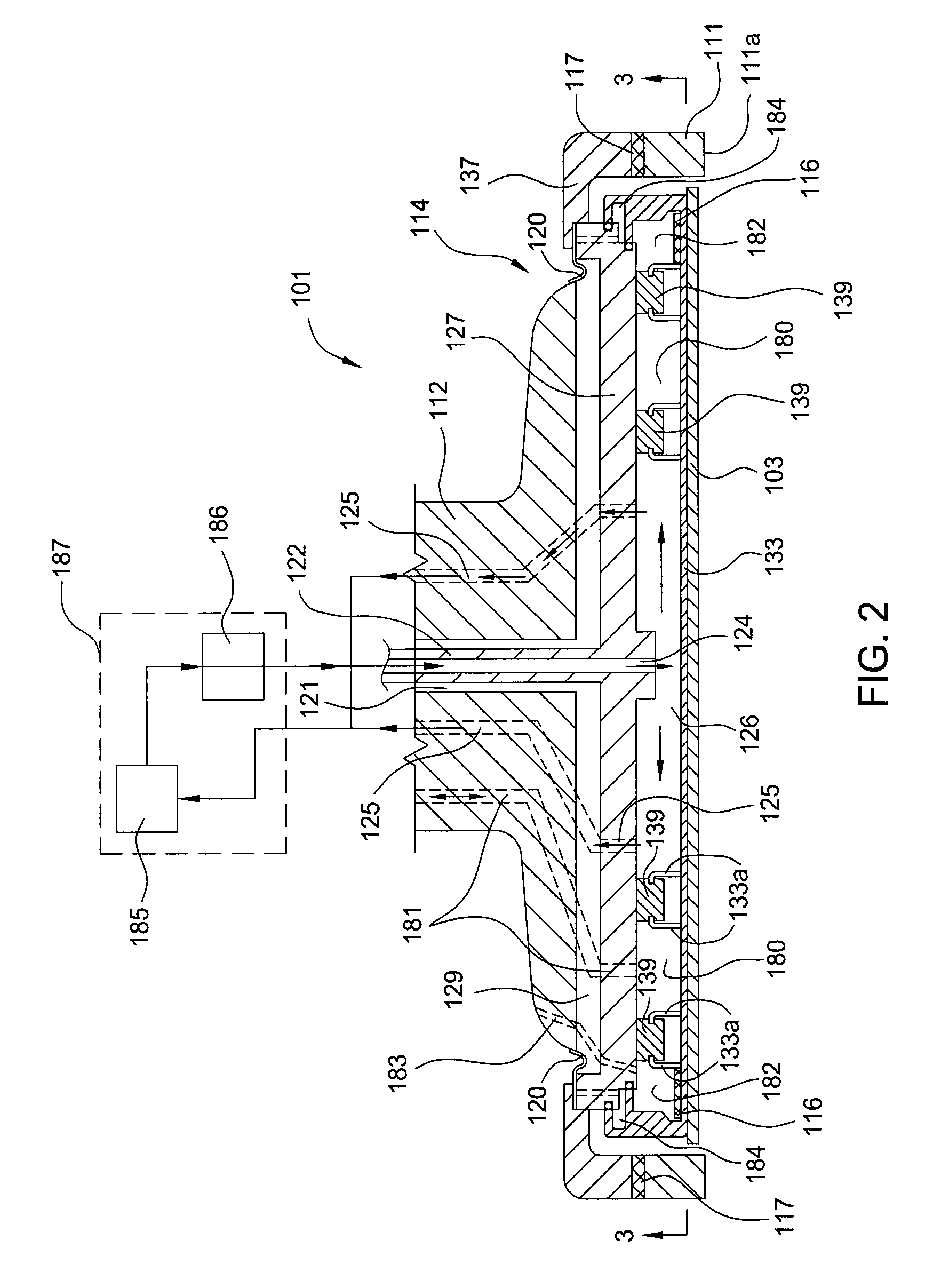
[0021]Embodiments of the present invention generally relate to an apparatus and a method for polishing a semiconductor substrate. Particularly, embodiments of the present invention relates to an apparatus and method for improving uniformity.

[0022]Embodiments of the present invention provide a heating mechanism configured to apply thermal energy to a perimeter of a substrate during polishing, or a cooling mechanism configured to cool a central region of the substrate during polishing, or a biased heating mechanism configured to create a temperature step differential on a given radius of a polishing pad.

[0023]One embodiment of the present invention provides a substrate carrier head having a heater disposed near an edge region of the substrate carrier head and a cooling mechanism disposed near a center region of the substrate carrier head. In another embodiment, the substrate carrier head comprises a retaining ring coupled to a retaining ring heater. Another embodiment of the present i...


PUM

PropertyMeasurementUnit
diameteraaaaaaaaaa
diameteraaaaaaaaaa
diameteraaaaaaaaaa

Abstract

Embodiments of the present invention relate to apparatus and method for improve uniformity of a polishing process. Embodiments of the present invention provide a heating mechanism configured to apply thermal energy to a perimeter of a substrate during polishing, or a cooling mechanism configured to cool a central region of the substrate during polishing, or a biased heating mechanism configured to create a temperature step differential on a given radius of a polishing pad.

Description

BACKGROUND OF THE INVENTION[0001]1. Field of the Invention[0002]Embodiments of the present invention generally relate to an apparatus and a method for polishing semiconductor substrates. More particularly, embodiments of the present invention provide apparatus and method for temperature control when polishing semiconductor substrates to improve uniformity.[0003]2. Description of the Related Art[0004]During fabrication of a semiconductor device, various layers, such as oxides, and copper, require planarization to remove steps or undulations prior to formation of subsequent layers. Planarization is typically performed mechanically, chemically, and / or electrically using processes such as chemical mechanical polishing (CMP), and electro-chemical mechanical polishing (ECMP).[0005]Chemical mechanical polishing typically includes mechanically abrading a substrate in a slurry that contains a chemically reactive agent. During chemical mechanical polishing, the slurry is delivered on a polish...

Claims


Application Information

Patent Timeline
Patent Type & Authority Applications(United States)
IPC IPC(8): B24B1/00B24B55/02B24B7/22B24B41/06
CPCB24B37/30B24B37/015H01L21/304
Inventor CHEN, HUNG CHIHHSU, SAMUEL CHU-CHIANGDANDAVATE, GAUTAM SHASHANKKOOSAU, DENIS M.
Owner APPLIED MATERIALS INC
Why Eureka
Try Eureka