Wiring board and method of manufacturing a semiconductor device

a semiconductor device and wire technology, applied in the field of wire boards, can solve the problems of not being able to form solder balls on the land warping in the thickness direction of the wire board, and not being able to reduce the stress/warp of printed circuits, so as to prevent the occurrence of deformation of the wire board and enhance the clamp area of the wire board

Inactive Publication Date: 2012-03-01
LONGITUDE SEMICON S A R L
View PDF3 Cites 7 Cited by
  • Summary
  • Abstract
  • Description
  • Claims
  • Application Information

AI Technical Summary

Benefits of technology

[0017]According to the present invention, because the wiring board comprises the second solid pattern that is provided in the clamp area, the rigidity o

Problems solved by technology

However, when a solid pattern is formed so as to continuously cover, in other words, completely cover, one face of a wiring board, there is the disadvantage that warping occurs in the thickness direction of the wiring board due to a difference in the coefficients of thermal expansion between the material forming the solid pattern and the material forming the wiring board.
Further, when a solid pattern is formed so as to completely cover one face of a wir

Method used


Image

  • Wiring board and method of manufacturing a semiconductor device
  • Wiring board and method of manufacturing a semiconductor device
  • Wiring board and method of manufacturing a semiconductor device

Examples


Embodiment Construction

[0027]The present invention will now be described herein with reference to illustrative embodiments. Those skilled in the art recognize that many alternative embodiments can be accomplished using the teachings of the present invention and that the present invention is not limited to the embodiments illustrated for explanatory purposes.

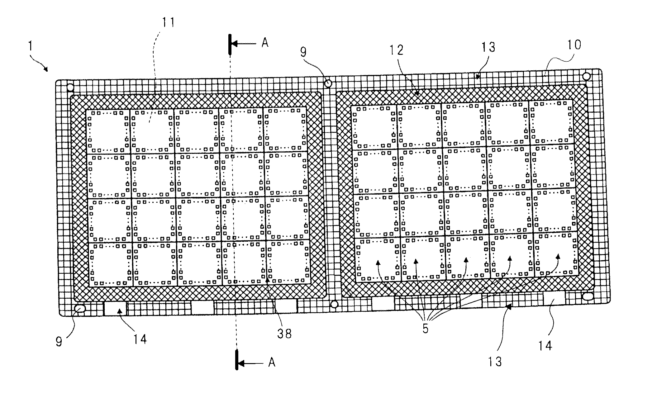
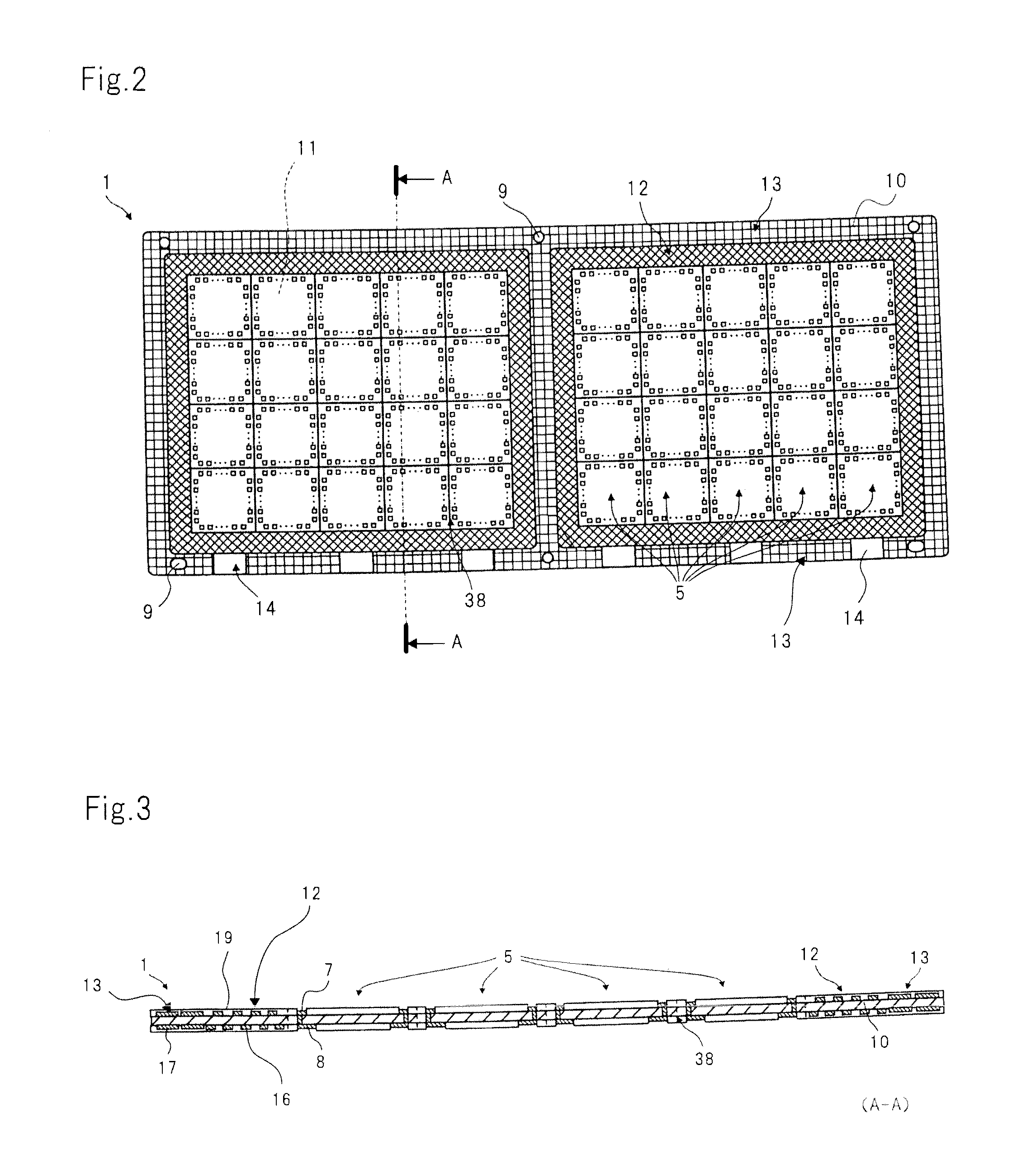
[0028]FIG. 2 shows a plan view of an outline configuration of a wiring board according to an exemplary embodiment. FIG. 3 shows a sectional view of the outline configuration of the wiring board according to the exemplary embodiment. FIG. 4 shows a plan view of the configurations of a first and a second solid pattern included in the wiring board according to the exemplary embodiment. FIG. 5 shows a plan view for describing the arrangement of dots comprising the first and second solid patterns according to the exemplary embodiment.

[0029]For example, a glass epoxy wiring board with a thickness of 0.1 mm is used as wiring board 1. As shown in FIG. 2, one s...


PUM


Abstract

A wiring board of this invention includes a product formation area in which are arranged a plurality of product formation sections on which a semiconductor chip is mounted; a molding area that is provided on an outer circumferential side of the product formation area, and with which a seal portion that covers the semiconductor chips mounted on the product formation sections makes contact; a clamp area that is provided on an outer circumferential side of the molding area, and that is held by a molding die that forms the seal portion; wiring that is provided in the product formation area, and that is electrically connected to the semiconductor chips; a first solid pattern that is provided in the molding area, and in which a plurality of dots are arranged; and a second solid pattern that is provided in the clamp area, and in which a plurality of dots that are larger than the dots of the first solid pattern are arranged.

Description

BACKGROUND OF THE INVENTION[0001]1. Field of the Invention[0002]The present invention relates to a wiring board on which semiconductor chips are mounted, and to a method of manufacturing a semiconductor device that uses the wiring board.[0003]2. Description of the Related Art[0004]Conventionally, a MAP (Mold Array Process) method is used as a method of manufacturing a BGA (Ball Grid Array) type semiconductor device. According to the MAP method, a semiconductor chip is mounted on each of a plurality of product formation sections defined on a wiring board, a sealing body that integrally covers the plurality of product formation sections is formed on the wiring board, and thereafter the wiring board is divided into respective product formation sections (for example, see JP2001-044324A or JP2001-044229A).[0005]A wiring board has a product formation area in which a plurality of product formation sections on which semiconductor chips are mounted are arranged, and a molding area on which a...

Claims


Application Information

Patent Timeline
IPC IPC(8): H05K1/00
CPCH01L21/561H01L2223/58H01L23/3142H01L23/49838H01L24/97H01L2224/48091H01L2224/48225H01L2224/48227H01L2224/97H01L2924/01029H01L2924/01079H05K1/0271H05K3/0097H05K3/284H05K3/4015H05K2203/041H05K2203/1316H01L21/565H01L2924/014H01L2924/01033H01L2924/01006H01L24/48H01L2924/01005H01L2924/00014H01L2224/85H01L2924/181H01L2924/00012H01L2224/45099H01L2224/45015H01L2924/207
Inventor KASHIWAYA, EMIKINDO, OSAMUSHIMADA, NORIOU
Owner LONGITUDE SEMICON S A R L
Why Eureka
Try Eureka