
Illuminating light communication device

Active Publication Date: 2012-03-01
PANASONIC INTELLECTUAL PROPERTY MANAGEMENT CO LTD
View PDF19 Cites 43 Cited by
  • Summary
  • Abstract
  • Description
  • Claims
  • Application Information

AI Technical Summary

Benefits of technology

[0014]It is an object of the present invention to provide an illuminating light communication device, of which a circuit added for communication can be simplified, which can faithfully modulate an outputted light in accordance with an optical communication signal having a high frequency.
[0016]According to the invention, a circuit added for communication can be simplified, and an outputted light can be faithfully modulated in accordance with an optical communication signal having a high frequency.

Problems solved by technology

Therefore, even as the light emitting diode needs little electricity, the benefit of the light emitting diode is diminished.
However, if the operating frequency of the DC-DC converter is relatively high, loss of the switching element Q1 in the DC-DC converter increases, and thus there is a problem that measures of noise-reduction are needed.
Therefore, it becomes difficult to modulate the load current I1 in accordance with the optical communication signal.
Thus, there is a problem that measures of noise from electric wiring are needed.
However, when the operating frequency increases, there is a problem that loss of the switching element Q1 also increases.
However, the feedback system becomes unstable and thereby abnormality oscillation may occur.
Therefore, there is a problem that it is difficult to modulate the load current I1 by changing a circuit constant of the phase compensation circuit added to the error amplifier A2.

Method used


Image

  • Illuminating light communication device
  • Illuminating light communication device
  • Illuminating light communication device

Examples


embodiment 1

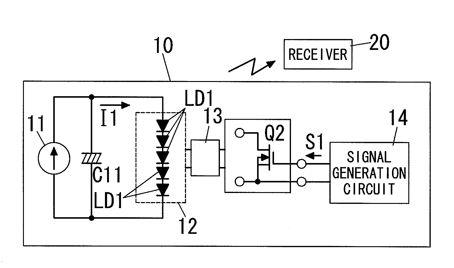
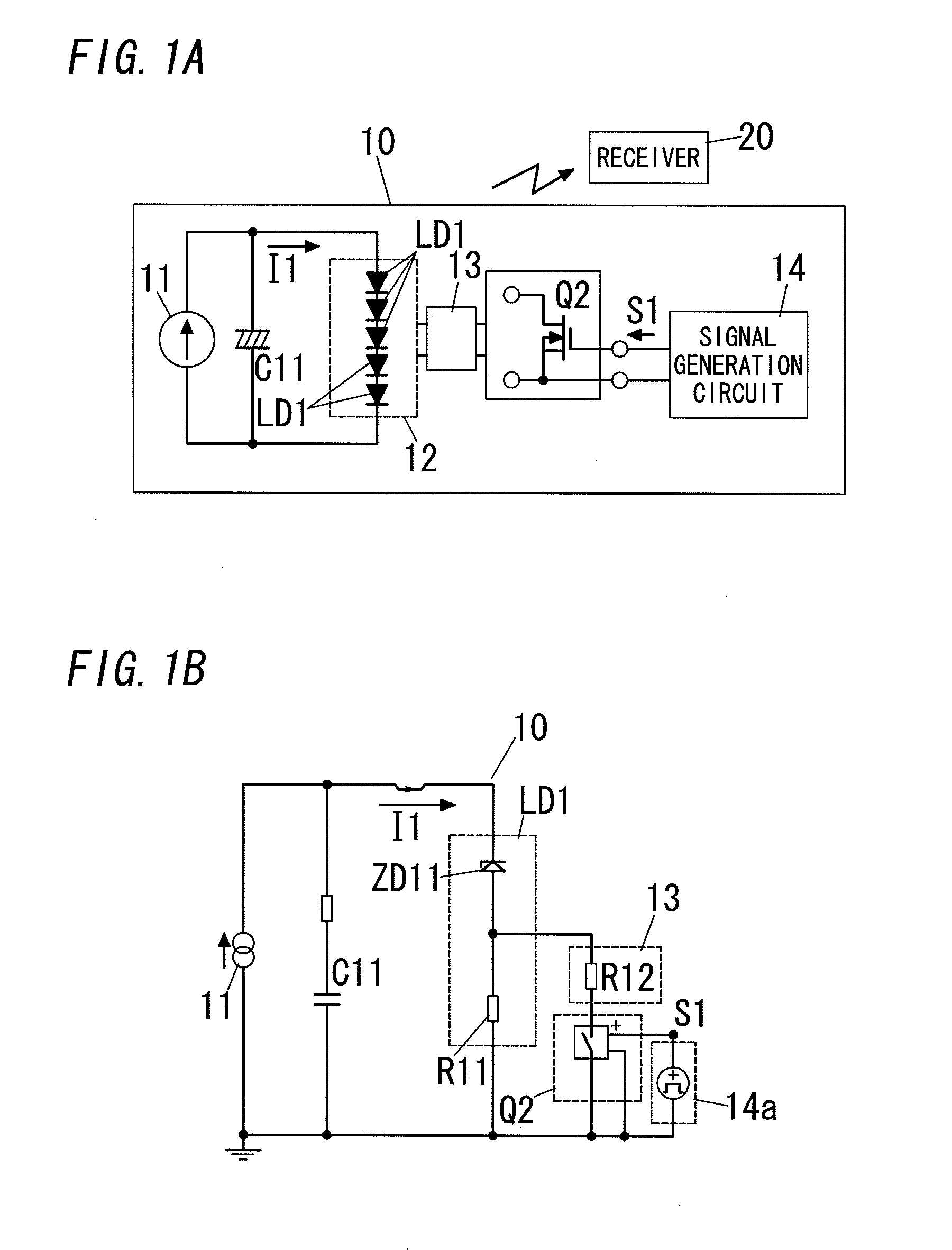
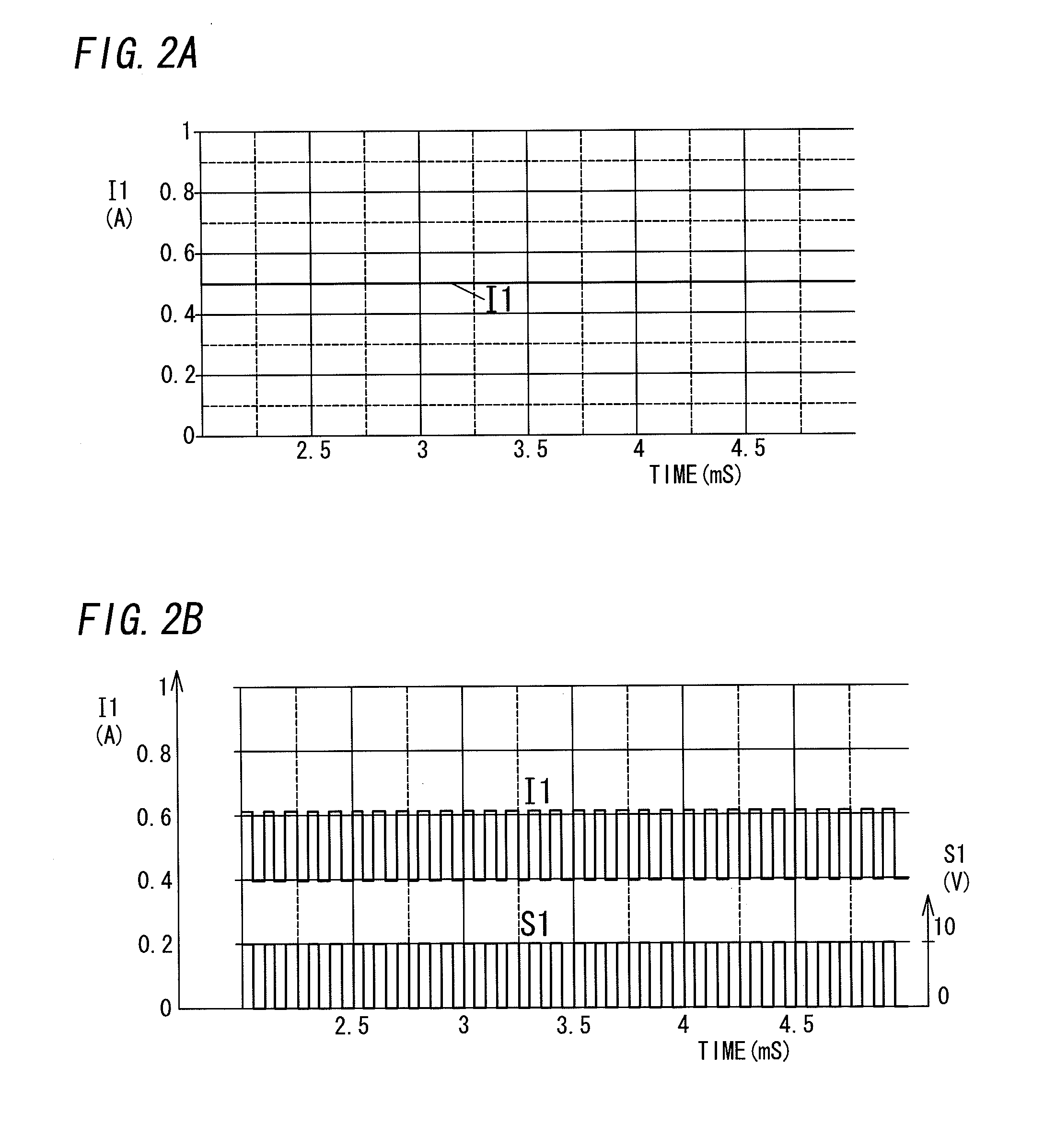
[0145]An illuminating light communication device of Embodiment 1 is explained with reference to FIGS. 1A and 1B. FIG. 1A is a circuit diagram for an illuminating light communication device 10. The illuminating light communication device 10 comprises a constant current source 11, a smoothing capacitor C11 (a smoothing circuit), a load circuit 12, a load change element 13, a signal generation circuit 14, and a switch element Q2.

[0146]The smoothing capacitor C11 is connected between outputs of the constant current source 11, and smoothes a power outputted from the constant current source 11.

[0147]The load circuit 12 comprises a plurality of light emitting diodes LD1, which are connected in series between the outputs of the constant current source 11, and receives the power outputted from the constant current source 11.

[0148]The load change element 13 is configured to partially change load characteristic of the load circuit 12, when being added to the load circuit 12. Then, for example,...

embodiment 2

[0157]An illuminating light communication device of Embodiment 2 is explained with reference to FIGS. 3A and 3B. FIG. 3A is a circuit diagram for an illuminating light communication device 10, and then the same code is referred to circuit components of FIG. 3A corresponding to circuit components of FIG. 1A, which was explained in the Embodiment 1, and the explanation is omitted. In the present embodiment, a plurality of light emitting diodes LD1 and a resistor R12 are connected between both ends of a smoothing capacitor C11, and a switch element Q2 is connected between both ends of the resistor R12. Here, the load change element 13 comprises the resistor R12 connected in series to the plurality of light emitting diodes LD1. Then, the switch element Q2 is switched on / off in accordance with the optical communication signal, and thereby the load change element 13 achieves the same effect as when load characteristic of the diodes LD1 is changed.

[0158]FIG. 3B is a circuit diagram modeled...

embodiment 3

[0162]An illuminating light communication device of Embodiment 3 is explained with reference to FIGS. 4A to 4E. An illuminating light communication device 10 of the present embodiment is different in only a configuration of the load change element 13 from the illuminating light communication device 10 which was explained in the Embodiment 1 or the Embodiment 2. Then, only the load change element 13 and the switch element Q2 are shown in FIGS. 4A to 4E, and other parts are omitted.

[0163]In the circuit of FIG. 4A, a diode D21 is used as the load change element 13, and the diode D21 is connected in series to the light emitting diode LD1. Then, a switch element Q2 is connected in parallel to the diode D21. When the switch element Q2 is switched on, short-circuiting is generated between both ends of the diode D21 through the switch element Q2 and then the diode D21 becomes not to be connected to the light emitting diode LD1. On the other hand, when the switch element Q2 is switched off, ...


PUM


Abstract

An illuminating light communication device comprises a constant current source, a smoothing capacitor connected to an output of the constant current source, a load circuit comprising a light emitting diode and connected to the output of the constant current source, a load change element added to the load circuit and thereby partially changing load characteristic of the load circuit, and a switch element configured to determine whether or not the load change element is added to the load circuit in accordance with a binary optical communication signal.

Description

TECHNICAL FIELD[0001]The present invention relates generally to illuminating light communication devices.BACKGROUND ART[0002]In the past, there have been proposed a lighting apparatus, which comprises a light emitting diode (LED) as a light source, and transmits a signal by modulating intensity of an illuminating light. Because such an illuminating light communication device transmits the signal by modulating the illuminating light itself, a special device such as an infrared-ray communication device is not required. Then, because the light emitting diode is used as the light source for illuminating, electric power saving can be implemented. Therefore, it has been studied that the illuminating light communication device is used for the ubiquitous information system in underground malls.[0003]FIG. 44 is a circuit diagram of the conventional illuminating light communication device. Then, a constant current circuit 52, three light emitting diodes 53, and a switching element Q1 are conn...

Claims


Application Information

Patent Timeline
IPC IPC(8): H04B10/04H05B37/02H05B44/00
CPCH04B10/1149H05B37/0272H04B10/116H05B47/195
Inventor NISHINO, HIROYUKISHIOHAMA, EIJIYAMASAKI, SHIGEAKI
Owner PANASONIC INTELLECTUAL PROPERTY MANAGEMENT CO LTD
Features
  • Generate Ideas
  • Intellectual Property
  • Life Sciences
  • Materials
  • Tech Scout
  • Unparalleled Data Quality
  • Higher Quality Content
  • 60% Fewer Hallucinations
Learn More