Semiconductor integrated circuit device

Inactive Publication Date: 2012-03-08
CANON KK
View PDF3 Cites 0 Cited by
  • Summary
  • Abstract
  • Description
  • Claims
  • Application Information

AI Technical Summary

Benefits of technology

[0005]The method described above of forming an electrically conductive pattern on a circuit block to be protected and detecting the change in potential of this electrically conductive pattern cannot accurately detect alterations to the

Problems solved by technology

The method described above of forming an electrically conductive pattern on a circuit block to be protected and detecting the change in potential of this electrically conductive pattern cannot accurately detect alterations to the electrically conductive pattern.

Method used


Image

  • Semiconductor integrated circuit device
  • Semiconductor integrated circuit device
  • Semiconductor integrated circuit device

Examples


Embodiment Construction

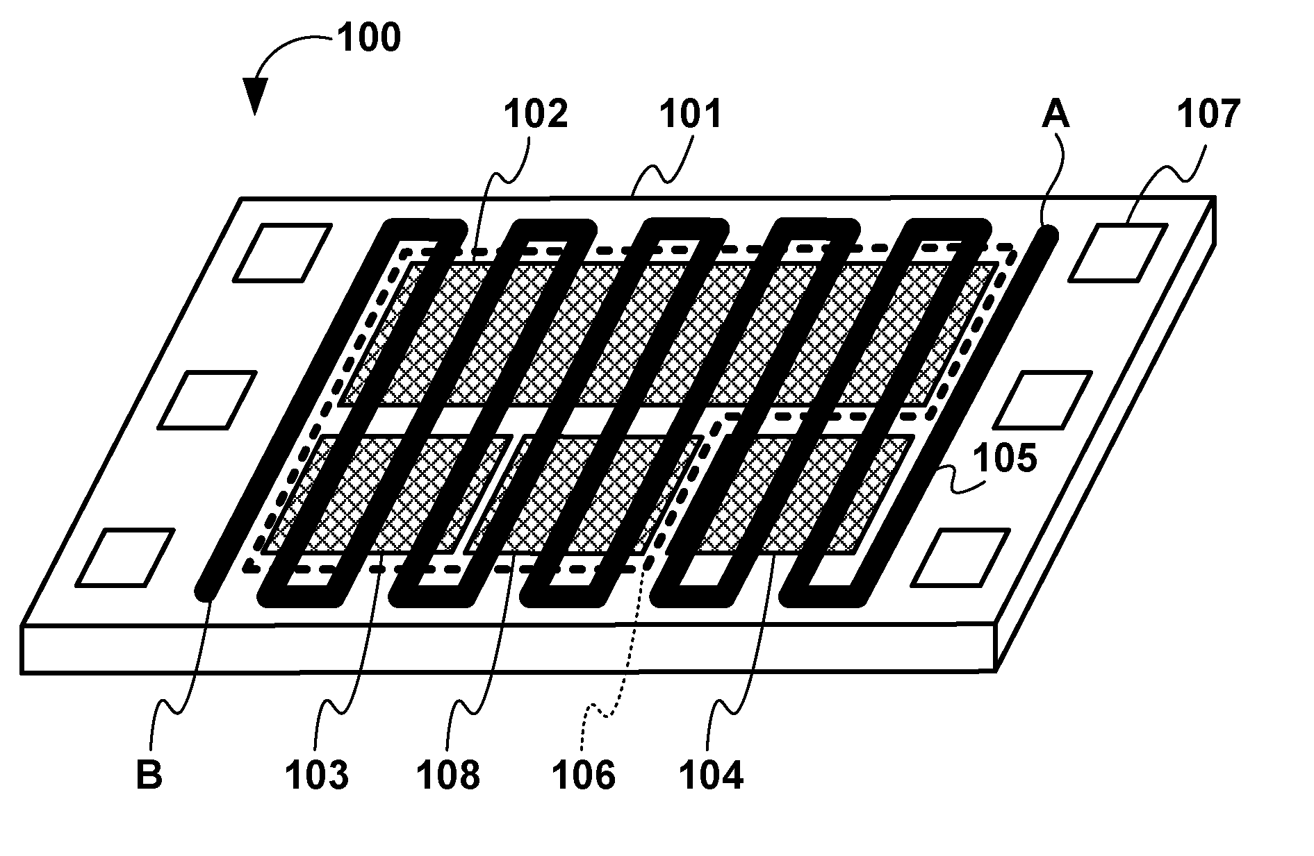
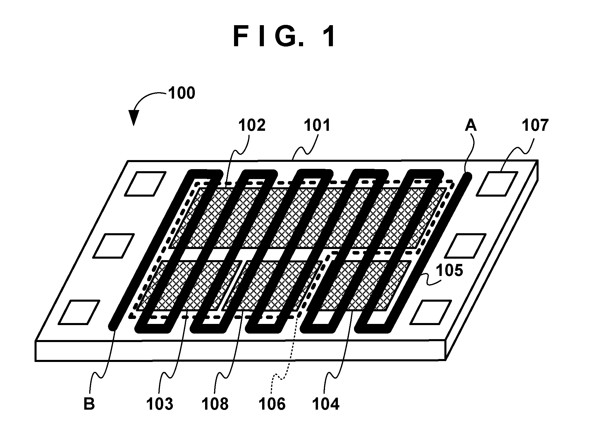
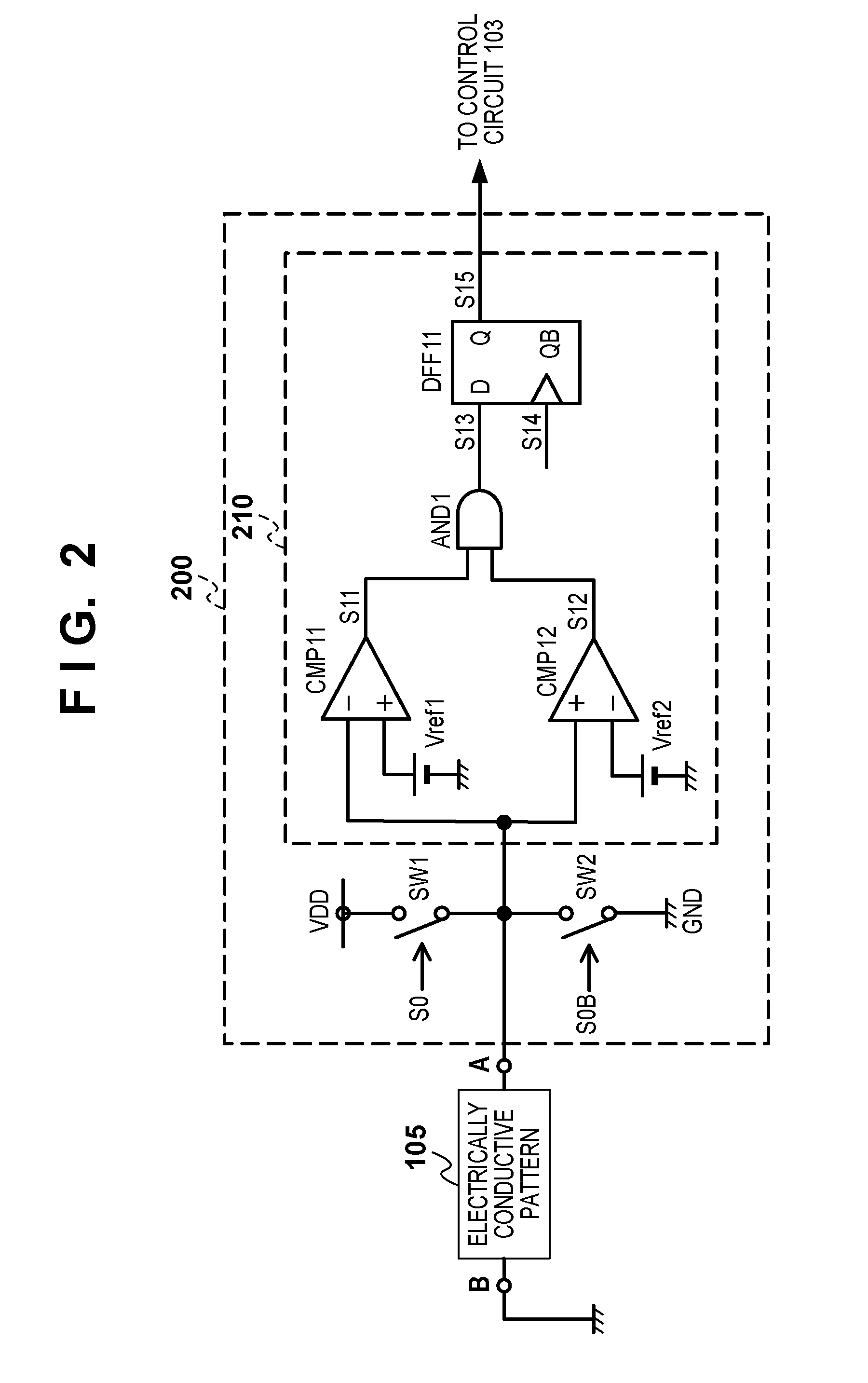
[0021]Embodiments of the present invention will be explained below with reference to the accompanying drawings. A configuration example of a semiconductor integrated circuit device 100 according to an embodiment of the present invention will now be explained with reference to FIG. 1. A semiconductor integrated circuit device 100 can include a memory circuit 102, control circuit 103, processing circuit 108, and detection circuit 104 formed over a semiconductor substrate 101. The memory circuit 102 can include at least one of a nonvolatile memory and volatile memory, and hold data. The control circuit 103 is, for example, a CMOS logic circuit, and can control access of the processing circuit 108 to data held in the memory circuit 102. That is, the control circuit 103 can control write of data to the memory circuit 102 by the processing circuit 108, and read of data from the memory circuit 102 by the processing circuit 108. The processing circuit 108 can process data held in the memory...


PUM


Abstract

A semiconductor integrated circuit device comprises: a circuit block formed on a semiconductor substrate; an electrically conductive pattern formed over a portion to be protected of the block; a resetting unit configured to reset a potential of a portion of the pattern to a reference potential; a connecting unit configured to connect the portion to a current supply line; and a detection circuit configured to determine whether a preset range includes a voltage of the portion when a predetermined time has elapsed since the portion is connected to the current supply line after the potential of the portion is reset to the reference potential is provided. A change in voltage of the portion depends on a circuit constant of the pattern.

Description

BACKGROUND OF THE INVENTION[0001]1. Field of the Invention[0002]The present invention relates to a semiconductor integrated circuit device.[0003]2. Description of the Related Art[0004]Demand has arisen for protecting, against physical alteration and analysis, a circuit mounted on a semiconductor integrated circuit device for holding data requiring high security such as personal information. In the semiconductor integrated circuit device described in Japanese Patent Laid-Open No. 2006-012159, a wiring line is formed on a circuit to be protected. When detecting a change in voltage of this wiring line, a detection circuit of the semiconductor integrated circuit device determines that the wiring line has been altered. However, a focused ion beam (FIB) apparatus has recently become usable. When using the FIB apparatus, it is possible to cut a wiring line by emitting an ion beam from the front surface of a semiconductor integrated circuit device, and deposit a wiring metal. Even when a ci...

Claims


Application Information

Patent Timeline
IPC IPC(8): G01R27/28
CPCH01L23/576H01L2924/0002H01L2924/00
Inventor OOMURA, MASANOBU
Owner CANON KK
Why Eureka
Try Eureka