
Method of fabricating semiconductor stack package

Inactive Publication Date: 2012-03-29
SAMSUNG ELECTRONICS CO LTD
View PDF8 Cites 99 Cited by
  • Summary
  • Abstract
  • Description
  • Claims
  • Application Information

AI Technical Summary

Benefits of technology

[0007]Thus, the inventive concept provides methods of fabricating a semiconductor stack package having a high capacity, a small volume and high reliability.

Problems solved by technology

When dies having the same size are stacked on a semiconductor substrate, it is difficult to secure an underfill space due to a narrow scribe line.

Method used


Image

  • Method of fabricating semiconductor stack package
  • Method of fabricating semiconductor stack package
  • Method of fabricating semiconductor stack package

Examples


Embodiment Construction

[0049]Hereinafter, the inventive concept will now be described more fully with reference to the accompanying drawing, in which exemplary embodiments of the inventive concept is shown. As the inventive concept allows for various changes and numerous embodiments, particular embodiments will be illustrated in the drawings and described in detail in the written description.

[0050]These embodiments are provided so that this disclosure will be thorough and complete, and will fully convey the scope of the invention to those skilled in the art. The inventive concept may, however, be embodied in many different forms and should not be construed as limited to the exemplary embodiments set forth herein.

[0051]The terms used herein are used to describe embodiments of the inventive concept, and not to limit the inventive concept. An expression used in the singular encompasses the expression of the plural, unless it has a clearly different meaning in the context. In the present specification, it is ...


PUM


Abstract

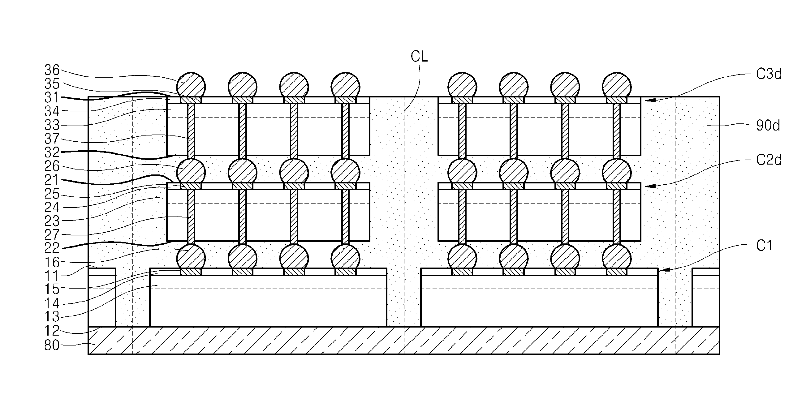
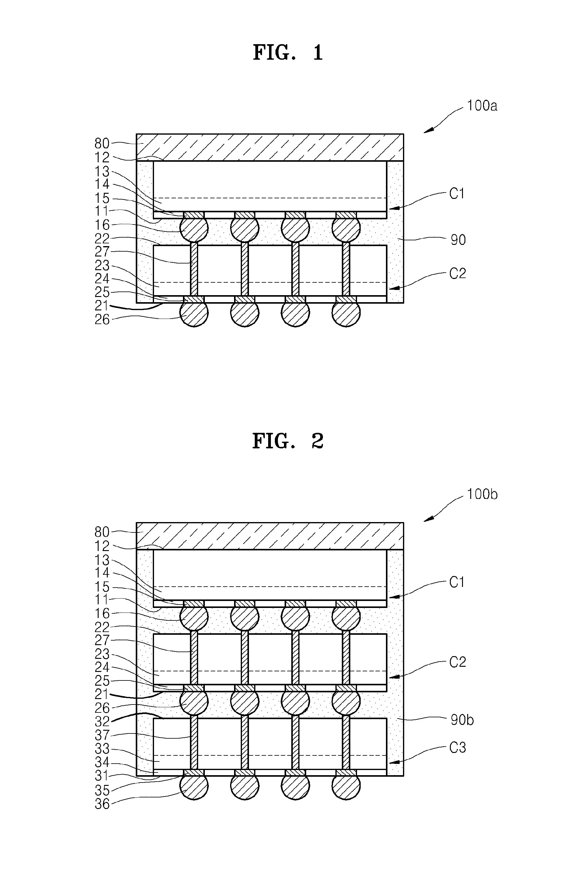
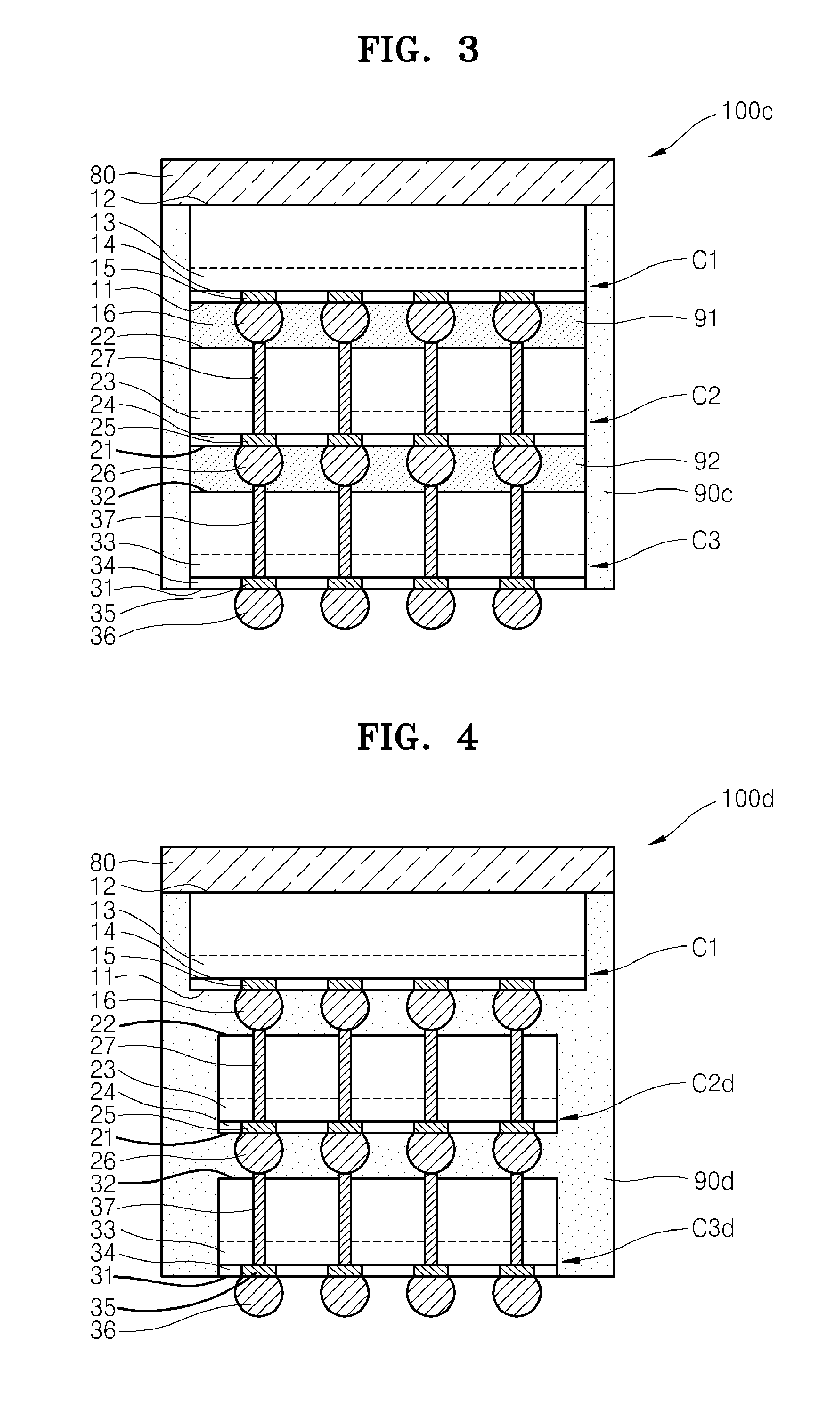
Methods of fabricating a semiconductor stack package having a high capacity, a small volume and reliability. According to the method of fabricating a semiconductor stack package, a first semiconductor substrate including a plurality of first semiconductor chips is attached to a chip protection film. The chip protection film is expanded such that the plurality of the first semiconductor chips are spaced apart from each other. A plurality of second semiconductor chips are attached to the plurality of the first semiconductor chips, respectively. A molding layer is formed between the plurality of the first semiconductor chips and between the plurality of the second semiconductor chips. The molding layer and the chip protection film are sawed to separate the semiconductor stack package comprising the first semiconductor chip and the second semiconductor chip into a unit.

Description

CROSS-REFERENCE TO RELATED APPLICATIONS[0001]This application claims the benefit of Korean Patent Application No. 10-2010-0093804, filed on Sep. 28, 2010, in the Korean Intellectual Property Office, the disclosure of which is incorporated herein in its entirety by reference.BACKGROUND OF THE INVENTION[0002]1. Field of the Invention[0003]The inventive concept relates to methods of fabricating a semiconductor stack package, and more particularly, to methods of fabricating a semiconductor package in which a plurality of semiconductor chips are stacked by using a through silicon via (TSV).[0004]2. Description of the Related Art[0005]Recently, as electronic devices become more integrated and smaller, semiconductor packages have been increasing in integration densities and performance and are smaller in size. In particular, a system in package including a logic chip and a memory chip as one package has been developed. There is still a need to develop a die stack package in which memory ch...

Claims


Application Information

Patent Timeline
IPC IPC(8): H01L21/98
CPCH01L25/0657H01L25/50H01L2224/16145H01L2225/06513H01L23/3107H01L2225/06541H01L2225/06582H01L2924/15311H01L2225/06517H01L2224/14181
Inventor PARK, SANG-SICKJANG, DONG-HYEONJEON, CHANG-SEONGLEE, TEAK-BOON
Owner SAMSUNG ELECTRONICS CO LTD
Learn More