Supercharge Your Innovation With Domain-Expert AI Agents!

Circuit board including embedded decoupling capacitor and semiconductor package thereof

Inactive Publication Date: 2012-04-05
SAMSUNG ELECTRONICS CO LTD
View PDF2 Cites 24 Cited by
  • Summary
  • Abstract
  • Description
  • Claims
  • Application Information

AI Technical Summary

Benefits of technology

[0010]Example embodiments provide a circuit board which can improve power integrity (PI).
[0011]Example embodiments also provide a semiconductor package which can improve power integrity (PI).

Problems solved by technology

In detail, mounting the decoupling capacitor on a surface of the main board may impose limitations on improvement of the PI characteristic because the decoupling capacitor is far from the semiconductor package.
In particular, in a case of a hand-held phone (HHP) in which various components are mounted on both surfaces of a main board, a decoupling capacitor may be mounted on one side of the main board, making it more difficult to improve the PI characteristic.
In a case of mounting the decoupling capacitor on a circuit board of a semiconductor package, the resulting structure may make the semiconductor package bulky, thus, such an arrangement may not be suitable for miniaturization of the semiconductor package.

Method used


Image

  • Circuit board including embedded decoupling capacitor and semiconductor package thereof
  • Circuit board including embedded decoupling capacitor and semiconductor package thereof
  • Circuit board including embedded decoupling capacitor and semiconductor package thereof

Examples


application examples

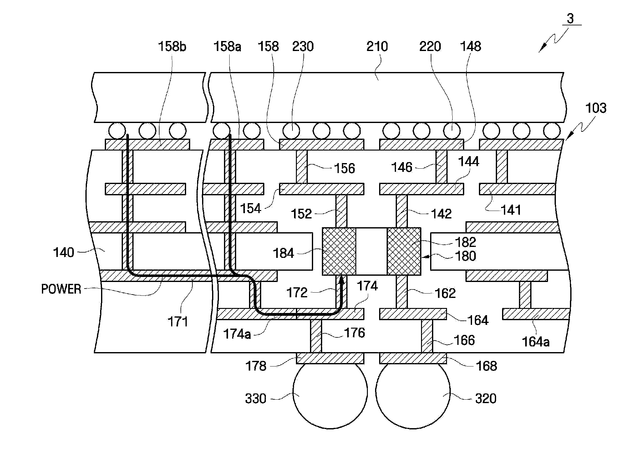
[0076]FIGS. 9 to 11 illustrate application examples of semiconductor packages according to example embodiments.

[0077]Referring to FIG. 9, the above-described semiconductor packages 1, 2, and 3, the circuit boards 101, 102, and 103 may be applied to a package module 1600 including various kinds of semiconductor devices. The package module 1600 may include a circuit board 1610 provided with a terminal 1640, a semiconductor chip 1620 mounted on the circuit board 1610, and a semiconductor chip 1630 packaged in a quad flat package (QFP) configuration. The semiconductor packages according to example embodiments may be applied to the semiconductor chips 1620 and 1630. The package module 1600 may be connected to an external electronic device through the terminal 1640.

[0078]Referring to FIG. 10, the above-described semiconductor packages 1, 2, and 3 may be applied to the electronic system 1700. The electronic system 1700 may include a controller 1710, an input and output (I / O) device 1720, a...


PUM


Abstract

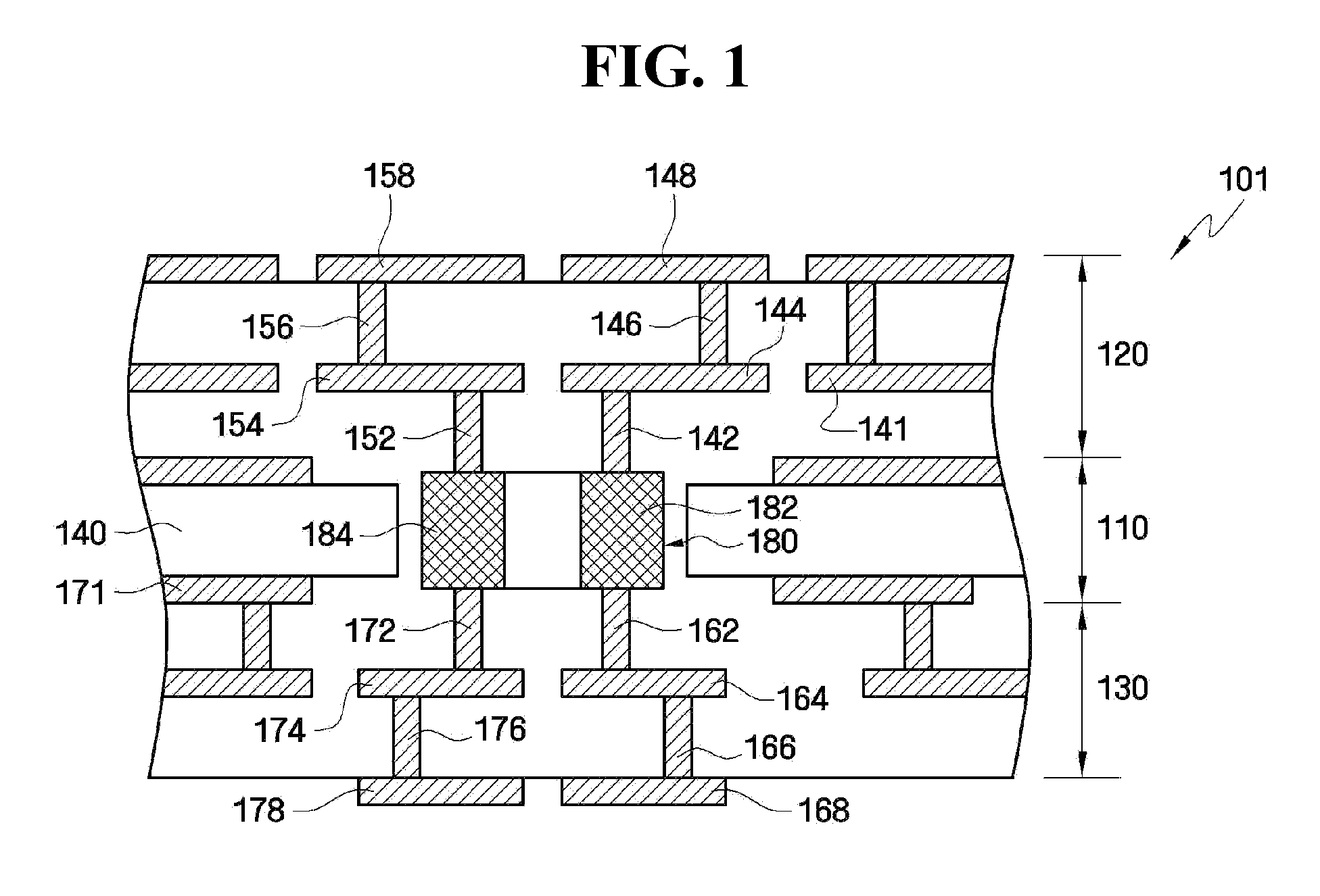
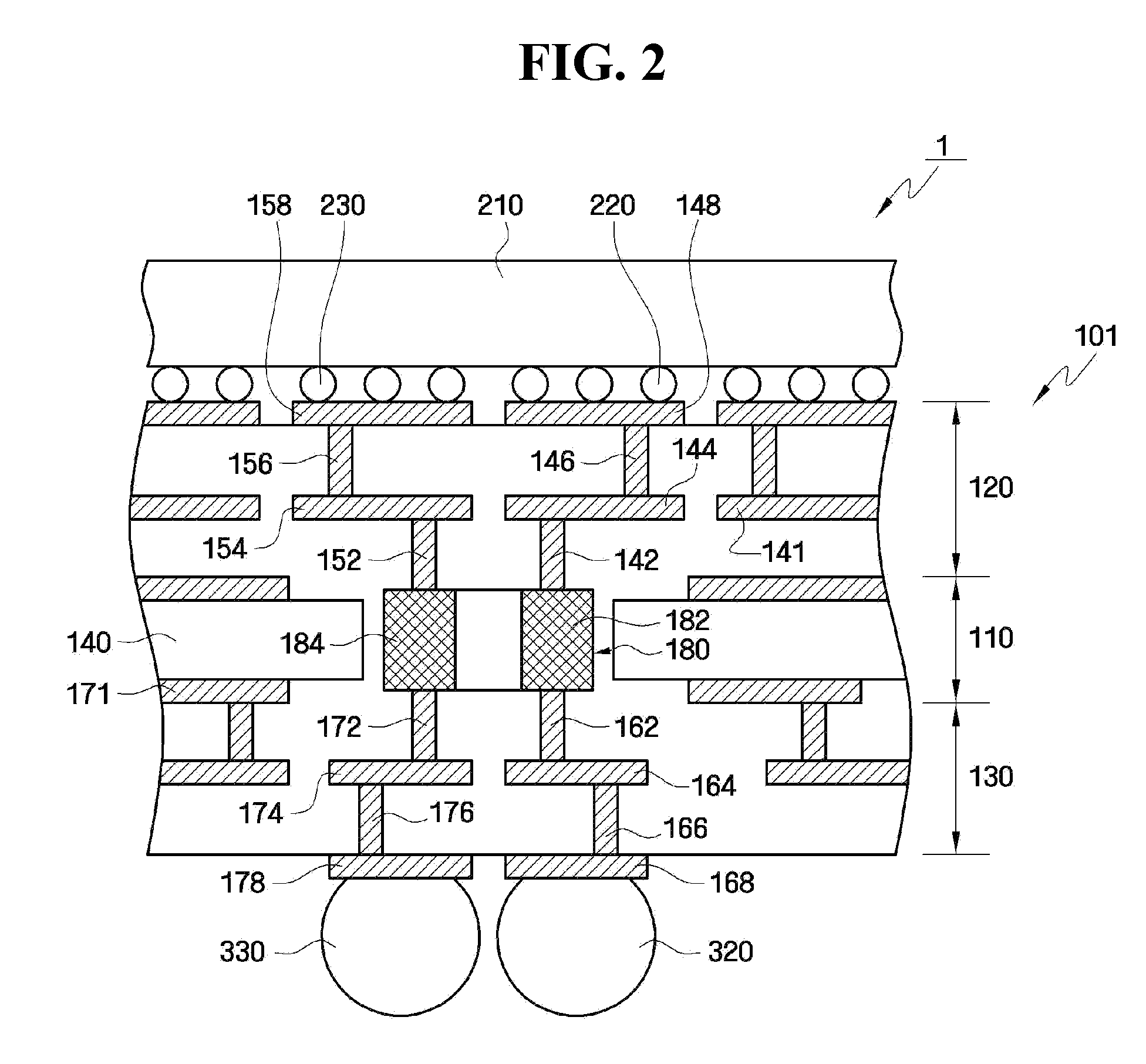
A circuit board including an embedded decoupling capacitor and a semiconductor package thereof are provided. The circuit board may include a core layer including an embedded decoupling capacitor, a first build-up layer at one side of the core layer, and a second build-up layer at the other side of the core layer, wherein the embedded decoupling capacitor includes a first electrode and a second electrode, the first build-up layer includes a first via contacting the first electrode, and the second build-up layer includes a second via contacting the first electrode.

Description

CROSS-REFERENCE TO RELATED APPLICATION[0001]This application claims priority under 35 U.S.C. §119 to Korean Patent Application No. 10-2010-0095924 filed on Oct. 1, 2010 in the Korean Intellectual Property Office, the entire contents of which are herein incorporated by reference.BACKGROUND[0002]1. Field[0003]Example embodiments relate to a circuit board including an embedded decoupling capacitor and a semiconductor package thereof.[0004]2. Description of the Related Art[0005]In order to improve characteristics of a semiconductor device, it is desirable to increase the speed of a memory controller and to improve power integrity (PI).SUMMARY[0006]A decoupling capacitor may be disposed at various locations of a semiconductor device. For example, the decoupling capacitor may be disposed on a main board in the form of a surface mounting capacitor (SMT) separately from a semiconductor package. Alternatively, the decoupling capacitor may be mounted on a surface of a circuit board of a semic...

Claims


Application Information

Patent Timeline
IPC IPC(8): H05K1/16
CPCH05K1/0231H05K1/185H01L2224/16225H01L24/17H05K3/4644H01L2924/15311
Inventor KIM, YONG-HOONLEE, HEE-SEOKLEE, JI-HYUN
Owner SAMSUNG ELECTRONICS CO LTD
Features
  • R&D
  • Intellectual Property
  • Life Sciences
  • Materials
  • Tech Scout
  • Unparalleled Data Quality
  • Higher Quality Content
  • 60% Fewer Hallucinations
Learn More