

Graphene oxide memory devices and method of fabricating the same
a graphene oxide and memory device technology, applied in bulk negative resistance effect devices, instruments, nanoinformatics, etc., can solve the problems of limited organic memory formed on flexible substrates, inability to maintain, and basic limitation of silicon-based memories that have not been overcom
- Summary
- Abstract
- Description
- Claims
- Application Information
AI Technical Summary
Problems solved by technology
Method used
Image

Examples
first embodiment
1. FIRST EMBODIMENT
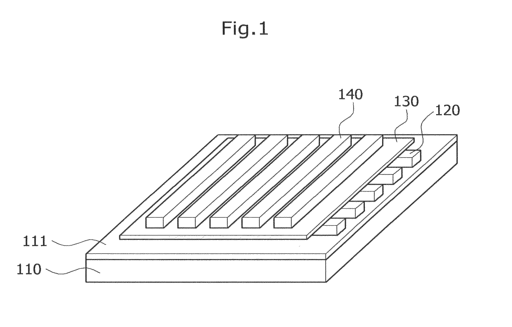
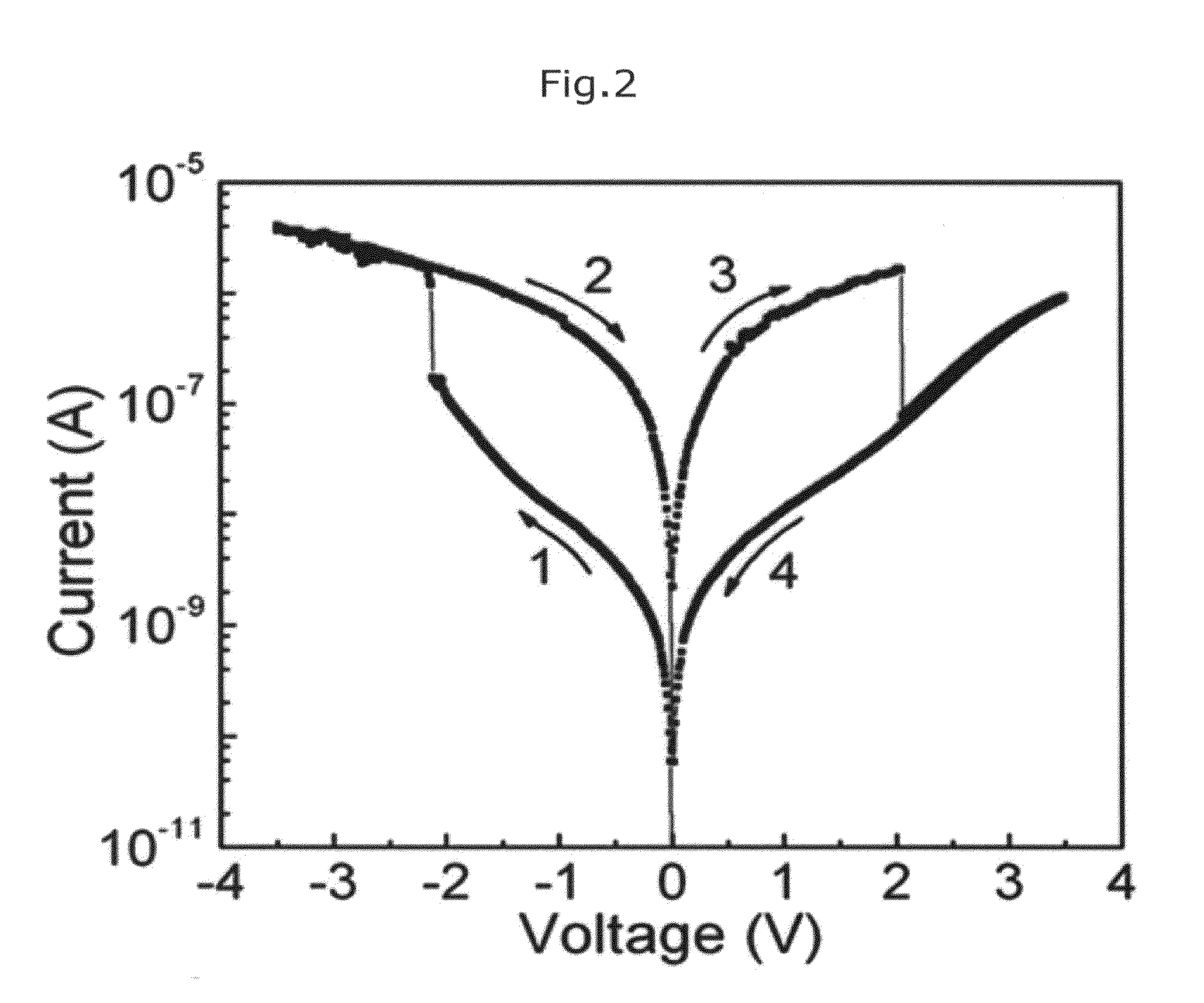
[0059]FIG. 1 illustrates a schematic view of a graphene oxide memory device according to a first embodiment of the present invention; FIG. 2 illustrates current-voltage characteristics of the graphene oxide memory device according to the first embodiment of the present invention; FIG. 3 illustrates log current-log voltage curves measured by applying a negative voltage according to the first embodiment of the present invention; and FIG. 4 illustrates log current-log voltage curves measured by applying a positive voltage according to the first embodiment of the present invention.
[0060]According to the first embodiment of the present invention, the graphene oxide memory device includes a graphene oxide thin film as an electron channel layer having electrical bistability.
[0061]In detail, the graphene oxide memory device of the first embodiment includes a substrate 110 coated with an insulating layer 111, lower electrodes 120 formed on the substrate 110, an electron ch...
second embodiment
2. SECOND EMBODIMENT
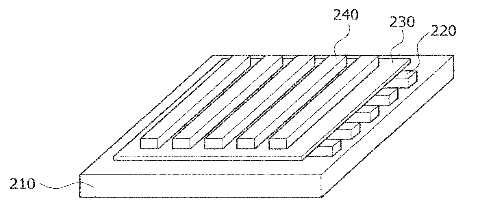
[0070]FIG. 5 illustrates a schematic view of a graphene oxide memory device according to a second embodiment of the present invention; FIG. 6 illustrates current-voltage characteristics of the graphene oxide memory device before and after the graphene oxide memory device is bent, according to the second embodiment of the present invention; FIG. 7 illustrates results of an Ion / Ioff repeatability test performed on the graphene oxide memory device according to the second embodiment of the present invention, and FIG. 8 illustrates results of an Ion state and Ioff state retention test performed on the graphene oxide memory device according to the second embodiment of the present invention.
[0071]As shown in FIG. 5, the graphene oxide memory device of the second embodiment includes an insulating substrate 210, lower electrodes 220 formed on the substrate 210, an electron channel layer 230 formed on the lower electrodes 220 by using a graphene oxide thin film, and upper ...
third embodiment
3. THIRD EMBODIMENT
[0078]FIG. 9 illustrates an image of a graphene oxide memory device captured after bending the graphene oxide memory device, according to a third embodiment of the present invention; FIG. 10 illustrates current-voltage characteristics of the graphene oxide memory device (AL / GO / AL / PES device) measured while increasing the number of bending cycles, according to the third embodiment of the present invention; FIG. 11 illustrates values of currents Ion and Ioff at a reading voltage of approximately −0.5 V with respect to the number of bending cycles according to the third embodiment of the present invention; FIG. 12 illustrates a schematic view of the AL / GO / AL / PES device and a measurement point of current-voltage characteristics, according to the third embodiment of the present invention; FIG. 13 illustrates current-voltage characteristics for different amounts of bending, according to the third embodiment of the present invention; and FIG. 14 illustrates values of cur...
PUM
 Abstract
Description
Claims
Application Information