Organic el lighting device and method of manufacturing the same

a lighting device and organic technology, applied in the direction of organic semiconductor devices, thermoelectric devices, solid-state devices, etc., can solve the problems of poor coating of organic functional layers in the taper portion of the barrier, uneven luminance in the plane due to voltage drop, and general poor light-emission unevenness, so as to facilitate the manufacture of organic el lighting devices and low cost

Inactive Publication Date: 2012-04-05
SEIKO EPSON CORP
View PDF13 Cites 25 Cited by
  • Summary
  • Abstract
  • Description
  • Claims
  • Application Information

AI Technical Summary

Benefits of technology

[0009]An advantage of some aspects of the invention is to provide an organic EL lighting device which suppresses the in-plane luminance unevenness due to a voltage drop and the generation of a local non-light emitting area due to a light-emission defect, and a method of manufacturing the organic EL lighting device.

Problems solved by technology

However, in an organic EL element which is formed in a wide planar area such as a backlight or a lighting device, since an ITO film or an IZO film which is used for a transparent electrode has a larger resistance than a metal film, in-plane unevenness in luminance due to a voltage drop occurs.
However, when an in-plane light-emission defect occurs, not only does light-emission unevenness due to a local non-light emitting area occur, most areas may not emit the light in accordance with the progression of the defect, whereby defective products may be produced.
With regard to the light-emission defect, the same problem also occurs in a light-emitting device which is constituted by a plurality of light-emitting pixels and has an auxiliary cathode formed on a barrier as in JP-A-2007-227129.
When the organic functional layer is formed on the first electrodes partitioned by the barriers, the coatability of the organic functional layer in a taper portion of the barrier is generally poor.
Accordingly, it becomes a cause of a short circuit between the first and second electrodes and a light-emission defect easily occurs.

Method used


Image

  • Organic el lighting device and method of manufacturing the same
  • Organic el lighting device and method of manufacturing the same
  • Organic el lighting device and method of manufacturing the same

Examples


first embodiment

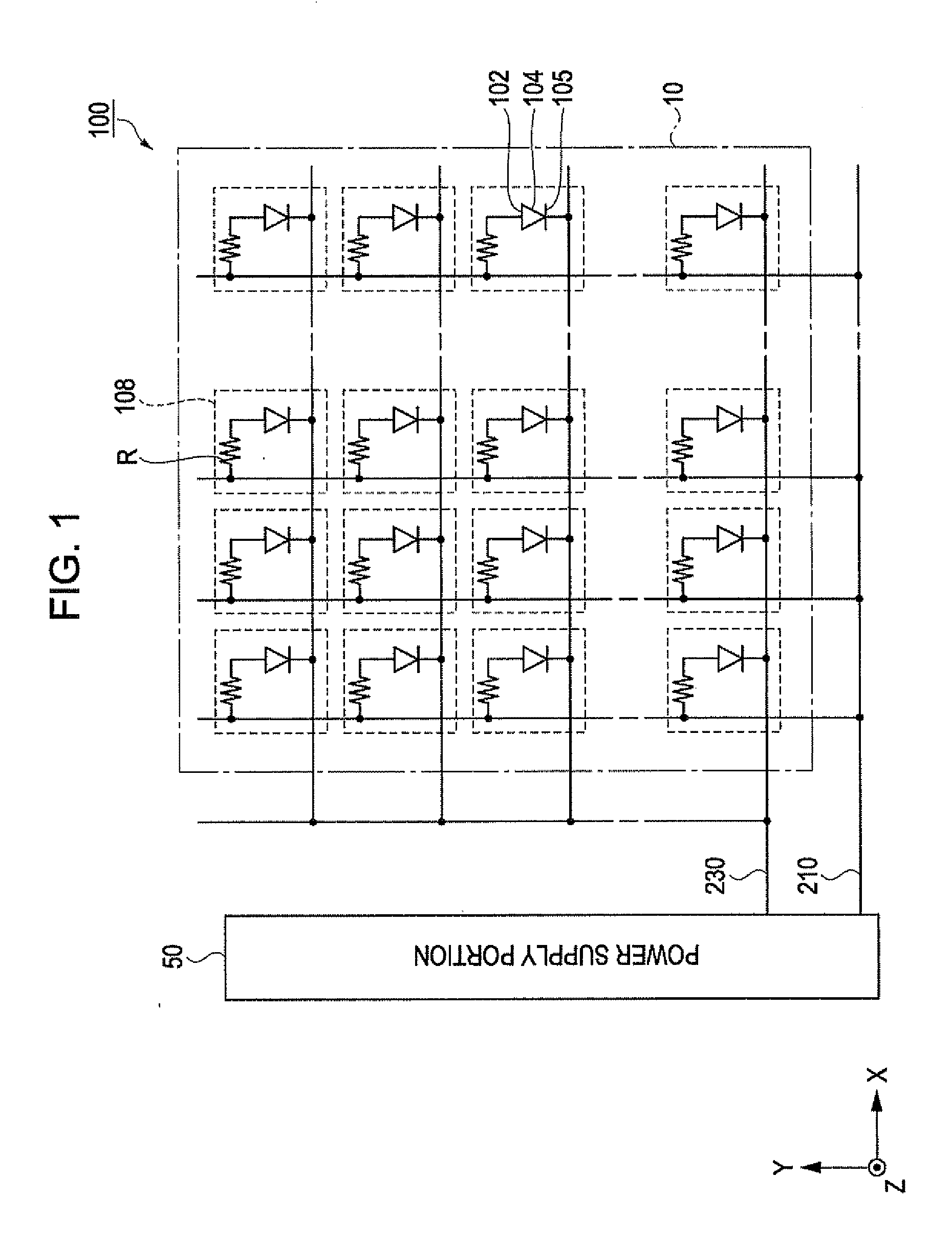
[0054]FIG. 1 is an equivalent circuit schematic of an organic EL lighting device according to a first embodiment.

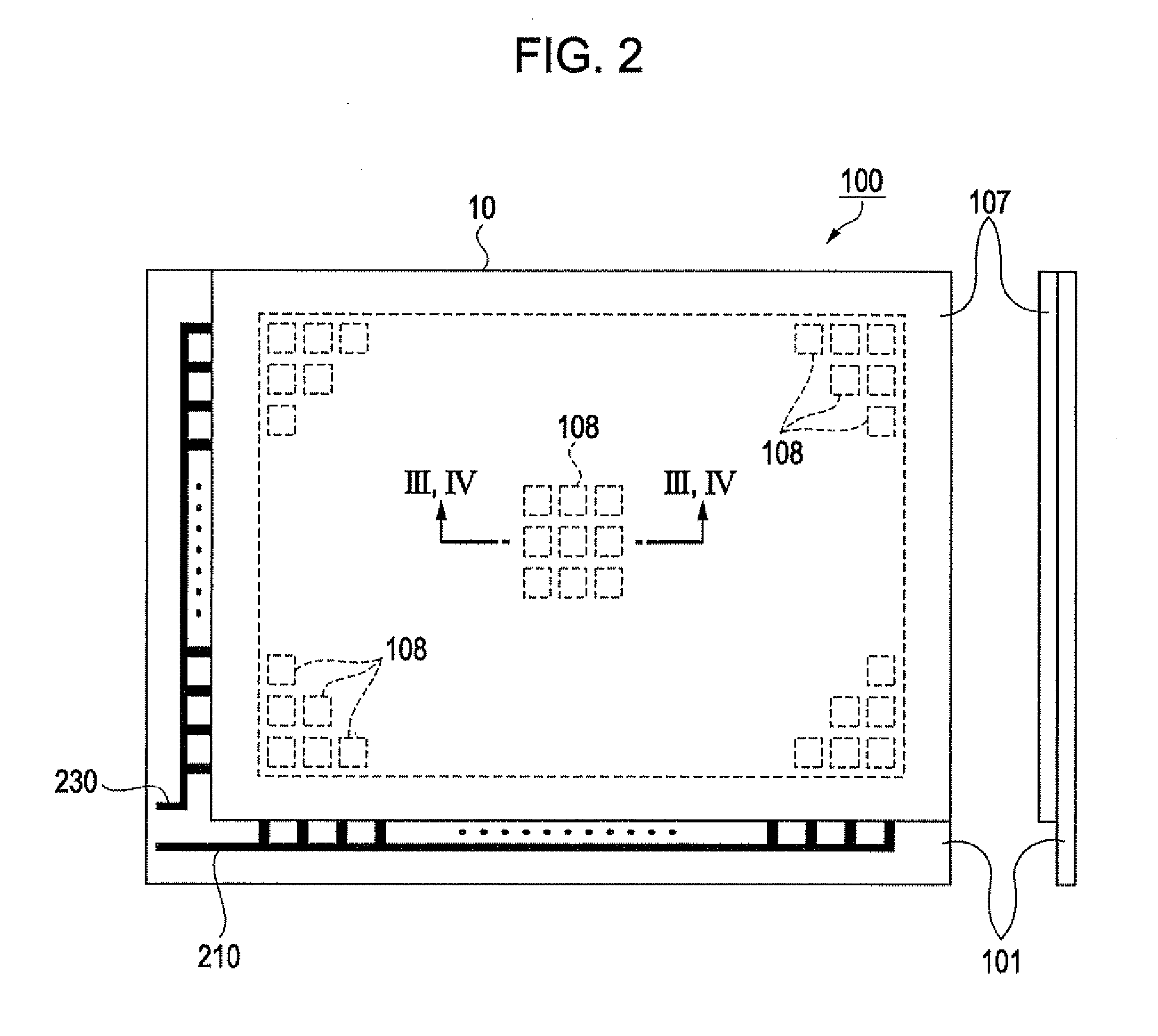
[0055]As shown in FIG. 1, an organic EL lighting device 100 of this embodiment has a lighting portion 10 and a power supply portion 50.

[0056]In the lighting portion 10, light-emitting portions (organic EL elements) 108 are formed in M columns×N rows (M and N are natural numbers equal to or larger than 1). Each of the plurality of light-emitting portions 108 is configured so that a first electrode 102, an organic functional layer 104 including a light-emitting layer, and a second electrode 105 are connected in series. In addition, a bleeder resistance R is connected to each light-emitting portion 108.

[0057]The power supply portion 50 supplies a high potential VH to the first electrode 102 via a first power wire 210, and supplies a low potential VL to the second electrode 105 via a second power wire 230. That is, the first electrode 102 functions as an anode and a second el...

second embodiment

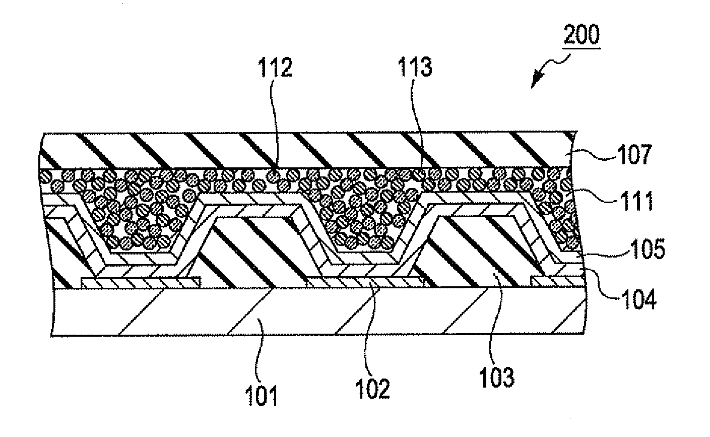
[0089]FIG. 5 is a cross-sectional view showing a configuration of an organic EL lighting device according to a second embodiment of the invention.

[0090]As shown in FIG. 5, an organic EL lighting device 200 of the second embodiment has the same configuration as in the first embodiment, except that a conductive / light-scattering layer 111 is constituted by two kinds of fine particles. Accordingly, the same constituent elements will be denoted by the same reference symbols and the detailed description thereof will be omitted.

[0091]The conductive / light-scattering layer 111 of the second embodiment is formed of transparent fine particles 112 and conductive fine particles 113. As in the first embodiment, light-permeable fine particles such as SiO2, TiO2 or ITO are used as the transparent fine particles 112, and thus the light-scattering property can be given to the conductive / light-scattering layer 111.

[0092]Furthermore, since the conductive / light-scattering layer 111 includes the conducti...

third embodiment

[0095]FIG. 6 is a cross-sectional view showing a configuration of an organic EL lighting device according to a third embodiment of the invention.

[0096]As shown in FIG. 6, in an organic EL lighting device 300 of the third embodiment, an organic layer 114 is divided by barriers 115. The other constituent elements are the same as in the first and second embodiments, but the description will be given using the constituent elements in the first embodiment as an example. The organic functional layer 114 is not formed in a continuous manner but formed independently for each of the light-emitting portions 108. Accordingly, deterioration when a defect occurs can be suppressed in units of the light-emitting areas in which the organic functional layer 114 is formed.

[0097]In general, in the case of a light-emission defect which occurs in an intrusion route of moisture and oxygen, the moisture and oxygen intruding through this route spread via the organic functional layer, and thus the light-emi...


PUM


Abstract

An organic EL lighting device includes a first electrode which is formed corresponding to each of the plurality of light-emitting portions on a substrate, an organic functional layer which is formed at least in a light-emitting area, a second electrode which is formed at least on the organic functional layer, and a conductive / light-scattering layer as a layer which has a conductive property and a light-scattering property, is formed on the second electrode, and is electrically connected to the second electrode. The conductive / light-scattering layer is formed of a conductive resin binder in which fine particles as transparent conductive fine particles are dispersed.

Description

BACKGROUND[0001]1. Technical Field[0002]The present invention relates to an organic EL lighting device and a method of manufacturing the organic EL lighting device.[0003]2. Related Art[0004]In recent years, organic EL devices having an electroluminescence (hereinafter, referred to as EL) element have attracted attention as a display device having a self light-emitting element. Organic EL devices have a configuration in which a light-emitting element in which a light-emitting layer made of an organic EL material is sandwiched between a pair of electrodes is provided in a substrate surface. Since the organic EL devices can be used in a display device such as a display or a thin planar light-emitting device, they are attracting attention as a backlight itself or a lighting device.[0005]Organic EL devices are classified into a bottom emission structure which extracts light from the side of a substrate and a top emission structure which extracts light from the side of an opposed substrat...

Claims


Application Information

Patent Timeline
Patent Type & Authority Applications(United States)
IPC IPC(8): H01L51/52H01L51/56
CPCH01L2251/5369H01L51/5268H10K50/854H10K2102/331
Inventor SEKI, SHUNICHI
Owner SEIKO EPSON CORP
Why Eureka
Try Eureka