Lens and method for manufacturing same

a technology of optical systems and lenses, applied in the field of optical systems, can solve the problems of reducing image quality, poor optical performance, and reducing image quality, and achieve the effects of reducing or completely avoiding aberration astigmatism, simple design, and reducing the cost of the optical system

Active Publication Date: 2012-04-05
FRAUNHOFER GESELLSCHAFT ZUR FOERDERUNG DER ANGEWANDTEN FORSCHUNG EV
View PDF5 Cites 30 Cited by
  • Summary
  • Abstract
  • Description
  • Claims
  • Application Information

AI Technical Summary

Benefits of technology

[0025]An advantage of the inventive approach is that it is now possible to manufacture wafer scale lenses with a design which does no longer have to take into consideration the glass substrate thickness. One further advantage is that by avoiding the optical unnecessary glass substrate (=parallel plates)

Problems solved by technology

This approach is disadvantageous as for mechanical and structural reasons the amount of high refractive index material, i.e. materials having a refractive index n of about 1.5 vs. n=1 of air, (e.g. the substrates which form parallel plates) within the imaging beam path is higher as it is desired by the optical design.
This reduces the image quality and necessitates more lenses and/or lenses having a more complicated shape within the stack to compensate for the reduced image quality.
Thus, the adaptation of “classic” lens designs and the use of the design rules which apply for these classic lens designs which avoid the occurrence of specific imaging errors cannot be used in the design of such wafer scale lenses.
However, this is contradiction to lens arrangements observed in classical objective designs where for example arrangements of one or several thin but strongly bent meniscuses are applied in order to reduce aberrations and especially to obtain a small astigmatism.
This is a drawback of state-of-the-art wafer scale lens designs as due to the evident problem of astigmatism in these designs their optical performance is poor although much more complex (highly aspheric) lens shapes are applied.
The problem of thick substrates is especially evident for the above mentioned meniscus lenses, which is the lens that has lens surfaces which are curved into the same direction.
In view of the strong curvature of the opposing surfaces of the meniscus a high thickness is necessitated so that the lens will lose its optical advantages.
However, this approach is disadvantageous, as

Method used


Image

  • Lens and method for manufacturing same
  • Lens and method for manufacturing same
  • Lens and method for manufacturing same

Examples


Embodiment Construction

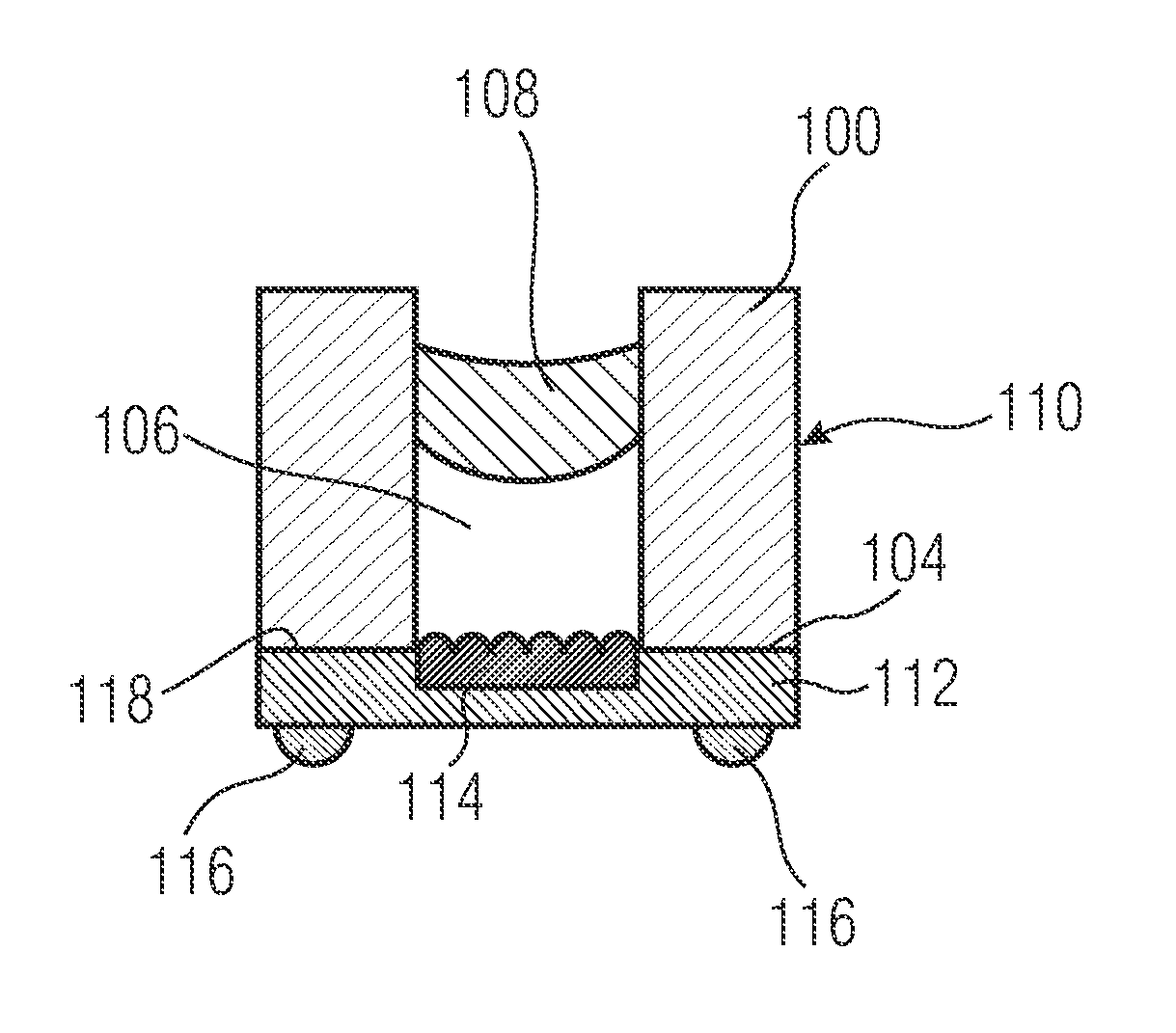
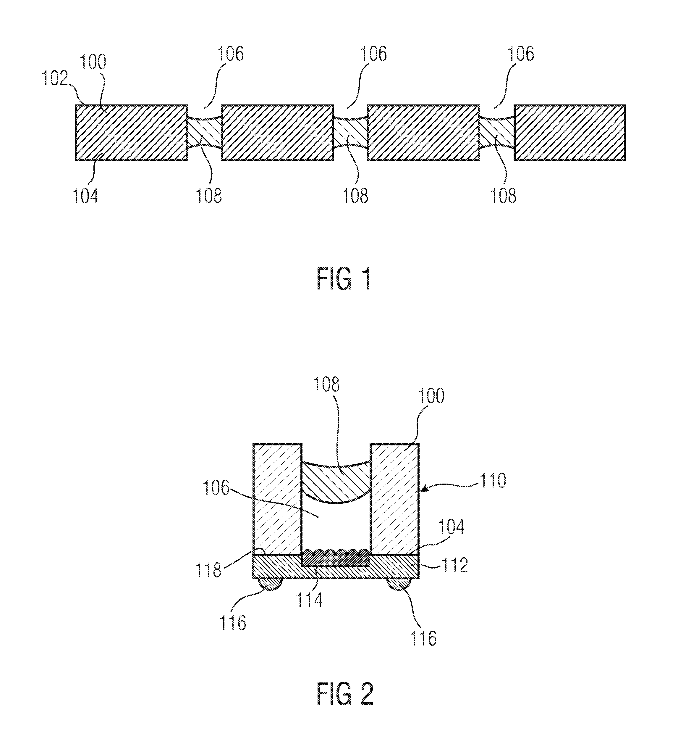
[0037]FIG. 1 illustrates an array of lenses in accordance with an embodiment of the invention. The lens array comprises a substrate or wafer 100 comprising two opposed main surfaces 102 and 104. The wafer 100 comprises a plurality of recesses 106 extending from the first surface 102 to the second surface 104 of the wafer 100, thereby defining a hole or opening through the wafer 100, also termed as cavity or spacer cavity. Within each recess or cavity 106 a lens structure 108 is arranged having the desired lens surfaces, in the embodiment shown in FIG. 1 a bi-concave lens. Alternatively, the lens structure 108 might have any desired type, e.g. a bi-convex lens, a plano-concave lens, a plano-convex lens or a meniscus. The lens structure 108 is formed of lens material and dependent from the desired characteristics the lens structure 108 may be formed by one or more layers of lens material. In case of using a plurality of layers of lens material dependent from the desired optical charac...


PUM

PropertyMeasurementUnit
Thicknessaaaaaaaaaa
Shapeaaaaaaaaaa

Abstract

In a method for manufacturing a lens, a substrate is provided which includes recess in a first surface thereof. A lens structure having a first desired lens surface and a second desired lens surface is formed in the substrate's recess.

Description

CROSS-REFERENCE TO RELATED APPLICATIONS[0001]This application is a continuation of copending International Application PCT / EP2009 / 003928, filed Jun. 2, 2009, which is incorporated herein by reference in its entirety.BACKGROUND OF THE INVENTION[0002]Embodiments of the invention concern the field of optical systems, more specifically the field of lenses and manufacturing such lenses. Embodiments of the invention relate to wafer scale optics, more specifically to wafer scale lens designs that may be used in lens arrangements or optical systems, e.g. in digital cameras in mobile phones, personal digital assistants and the like, especially in combination with CMOS image sensors.[0003]In the field of wafer scale optics lenses are manufactured by providing a UV curable polymer material onto a thick glass substrate and shaping the polymer material into a desired lens form. The polymer may be deposited either on one side or on both sides of the glass substrate. A plurality of such lens wafer...

Claims


Application Information

Patent Timeline
IPC IPC(8): B29D11/00G02B7/02
CPCB29D11/00375B29C33/52B29D11/00307
Inventor DUPARRE, JACQUESWIPPERMANN, FRANKDANNBERG, PETERBRAEUER, ANDREAS
Owner FRAUNHOFER GESELLSCHAFT ZUR FOERDERUNG DER ANGEWANDTEN FORSCHUNG EV
Why Eureka
Try Eureka