Array substrate of display panel and method of repairing the same

a display panel and substrate technology, applied in the field of display panel substrate array, can solve the problems of deterioration of display quality, increased probability of defects in gate line fabrication, data line or other conducting pattern, and increase of rc loading of repairing segment, so as to achieve the effect of improving display quality and not increasing rc loading

Active Publication Date: 2012-04-12
AU OPTRONICS CORP
View PDF6 Cites 8 Cited by
  • Summary
  • Abstract
  • Description
  • Claims
  • Application Information

AI Technical Summary

Benefits of technology

[0005]It is therefore one of the objectives of the present invention to provide an array substrate of a display panel and a method of repairing the same to decrease the RC loading of the repairing segment of the array substrate.
[0008]The method of repairing an array substrate of a display panel of the present invention uses a part of the common line as the substitution line of the data line with a broken line defect so that the RC loading will not be increased and the display quality is effectively improved after repairing. Moreover, it is not necessary to reserve the layout space in the peripheral region for disposing the repairing lines, and therefore the design of slim boarder can be accomplished.

Problems solved by technology

Under this condition, the probability of defects is also increased in the fabrication of gate lines, data lines or other conducting patterns of the array substrate.
However, because the repairing segments are disposed on the peripheral region of the array substrate, the RC loading of the repairing segment will increase due to its excessive long path.
Consequently, the quality of display is deteriorated.
Furthermore, enough space should be maintained in the peripheral region of the array substrate for disposing the repairing segments, which makes it impossible to accomplish the design of slim boarder for the conventional liquid crystal display panel.

Method used


Image

  • Array substrate of display panel and method of repairing the same
  • Array substrate of display panel and method of repairing the same
  • Array substrate of display panel and method of repairing the same

Examples


Embodiment Construction

[0013]To provide a better understanding of the present invention, preferred embodiments will be made in detail. The preferred embodiments of the present invention are illustrated in the accompanying drawings with numbered elements.

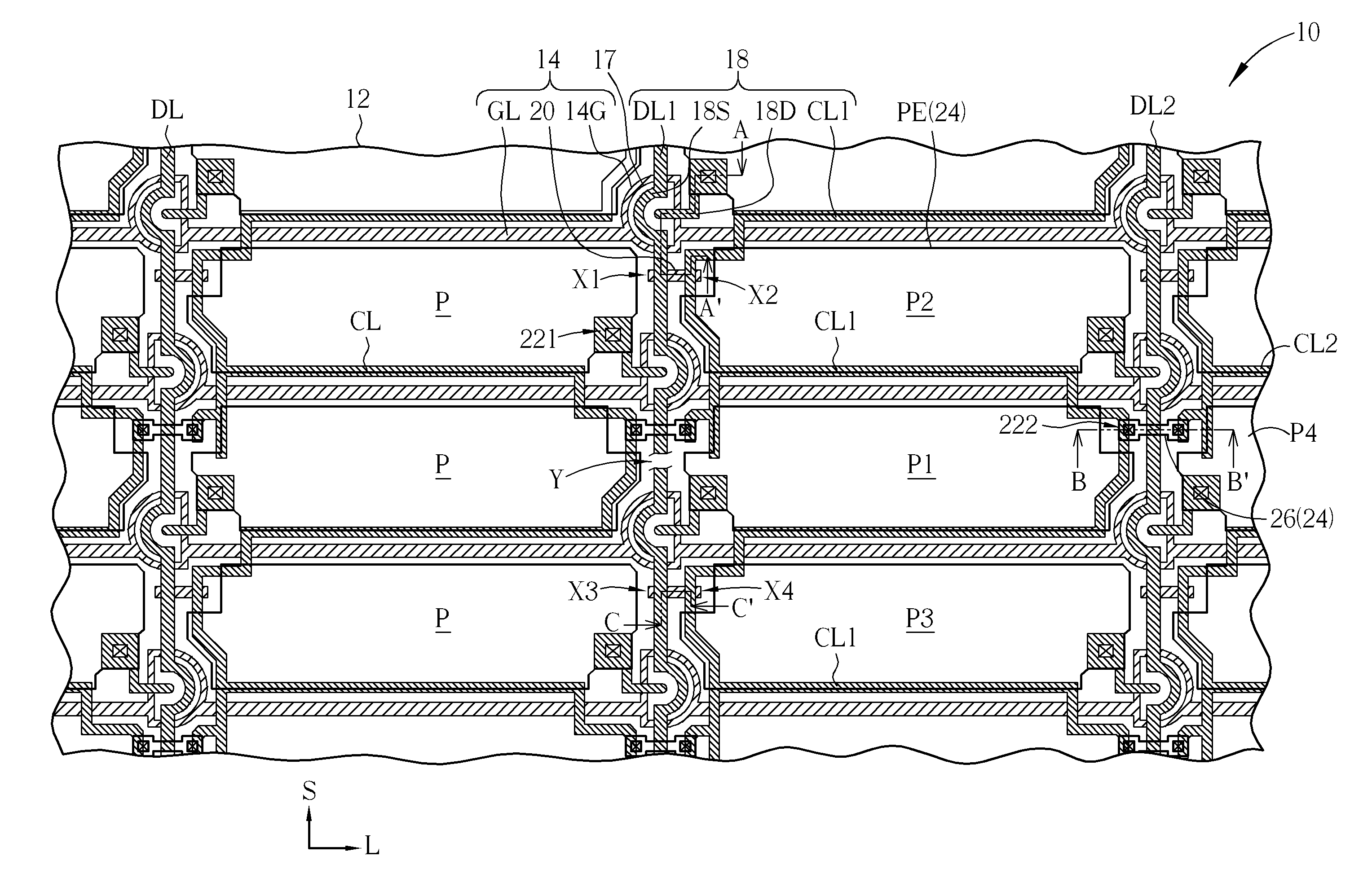
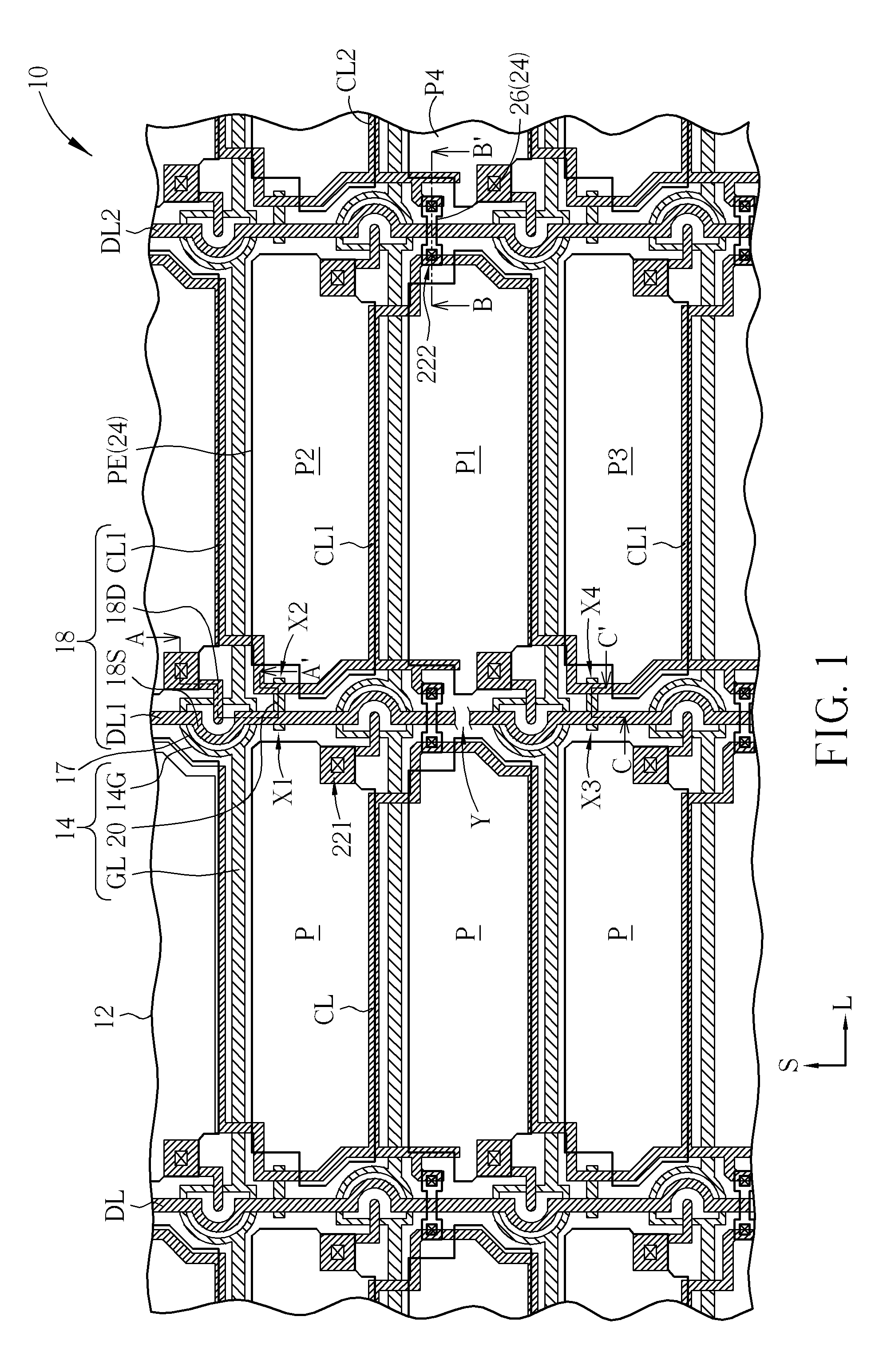
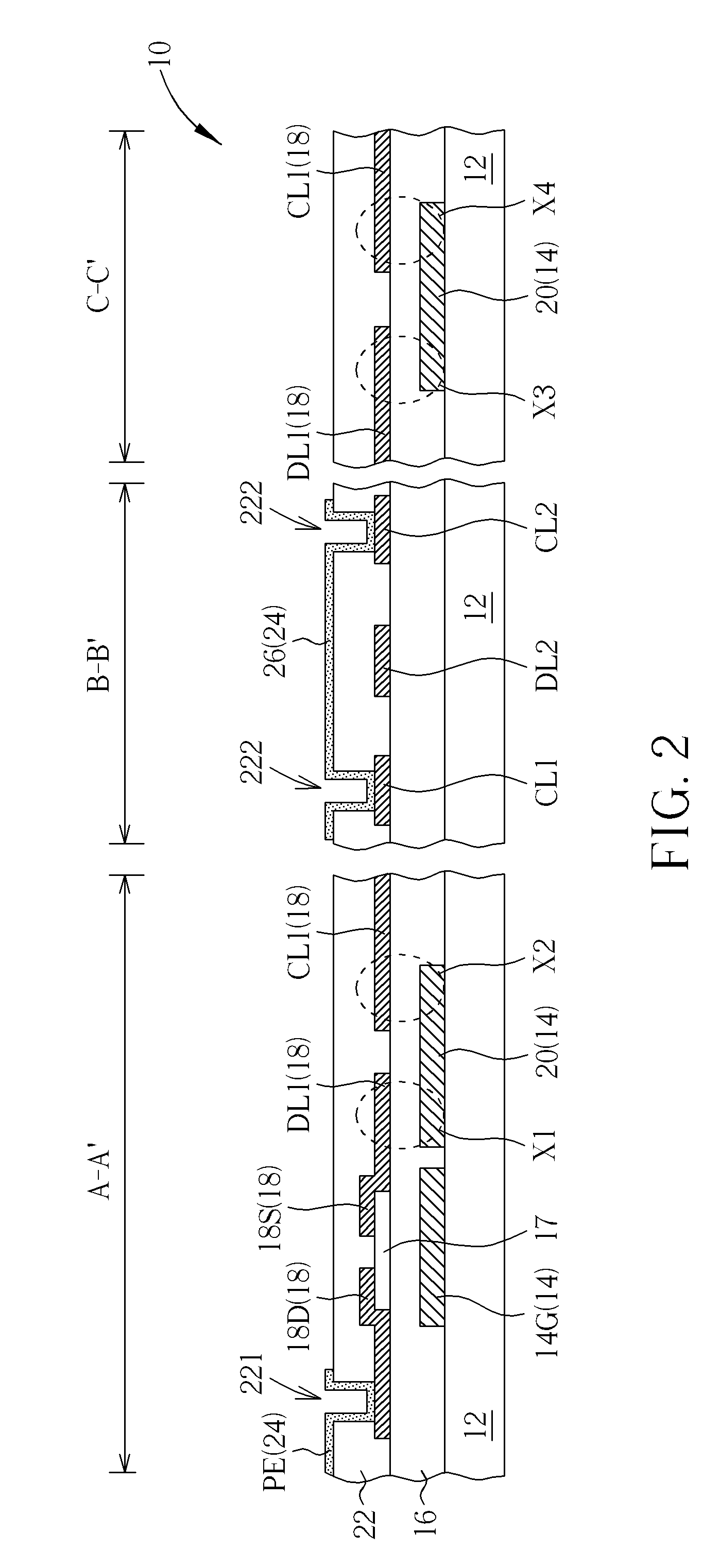
[0014]Please refer to FIGS. 1-4. FIGS. 1-4 illustrate a method of repairing an array substrate of a display panel according to a first embodiment of the present invention. FIG. 1 and FIG. 3 are top views of the array substrate of the display panel, FIG. 2 is a cross-sectional view of the array substrate of the display panel taken along lines A-A′, B-B′ and C-C′ in FIG. 1, and FIG. 4 is a cross-sectional view of the array substrate of the display panel taken along lines A-A′, B-B′ and C-C′ in FIG. 3. In this embodiment, the display panel could be any kinds of liquid crystal display panels. As shown in FIG. 1 and FIG. 2, an array substrate 10 (also known as thin film transistor substrate, TFT substrate) is provided. The array substrate 10 includes a substrat...


PUM

PropertyMeasurementUnit
areaaaaaaaaaaa
areaaaaaaaaaaa
transparentaaaaaaaaaa

Abstract

A method of repairing array substrate of display panel includes the following steps. An array substrate including a substrate, gate lines, data lines, common lines and repairing segments is provided. The gate lines and the data lines are intersected to define a plurality of pixel areas. The data lines include a first data line. The common lines include a first common line. The first data line has a broken line defect. A cutting process is performed to form a first cutting part and a second cutting part on the first common line, and thus the first common line between the first cutting part and the second cutting part forms a floating common repairing segment. A connecting process is performed to electrically connect the repairing segments, the first data line and the common repairing segment, so that the common repairing segment serves as a substitution line of the first data line.

Description

BACKGROUND OF THE INVENTION[0001]1. Field of the Invention[0002]The present invention relates to an array substrate of a display panel and a method of repairing the same, and more particularly, to an array substrate of a display panel with low resistance-capacitance loading (RC loading) and high display quality, and a method of repairing the same.[0003]2. Description of the Prior Art[0004]Display panels, such as liquid crystal display panels, are mainly constructed by an array substrate, a color filter substrate, and liquid crystal molecules filled between the two substrates. A plurality of devices, such as a plurality of pixel areas arranged in array, gate lines, data lines, common lines, and thin film transistors, are disposed on the array substrate. As the application of liquid crystal display device prevails, the requirements for high resolution and high aperture ratio are also increased. In order to satisfy the specification of high resolution and high aperture ratio, the width...

Claims


Application Information

Patent Timeline
Patent Type & Authority Applications(United States)
IPC IPC(8): G02F1/1333H01R43/00
CPCG02F1/136259G02F2001/136263Y10T29/49155Y10T29/49117Y10T29/49718H01L27/156G02F1/136263
Inventor WU, YEN-FENG
Owner AU OPTRONICS CORP
Why Eureka
Try Eureka