Transistor having notched fin structure and method of making the same

a technology of transistors and fins, applied in the direction of basic electric elements, electrical equipment, semiconductor devices, etc., can solve the problems of premature breakdown of the finfet, and the challenges of the current finfet technology

Active Publication Date: 2012-04-12
TAIWAN SEMICON MFG CO LTD
View PDF7 Cites 152 Cited by
  • Summary
  • Abstract
  • Description
  • Claims
  • Application Information

AI Technical Summary

Problems solved by technology

Current FinFET technology, however, has challenges.
The effect is premature breakdown of the FinFET.

Method used


Image

  • Transistor having notched fin structure and method of making the same
  • Transistor having notched fin structure and method of making the same
  • Transistor having notched fin structure and method of making the same

Examples


Embodiment Construction

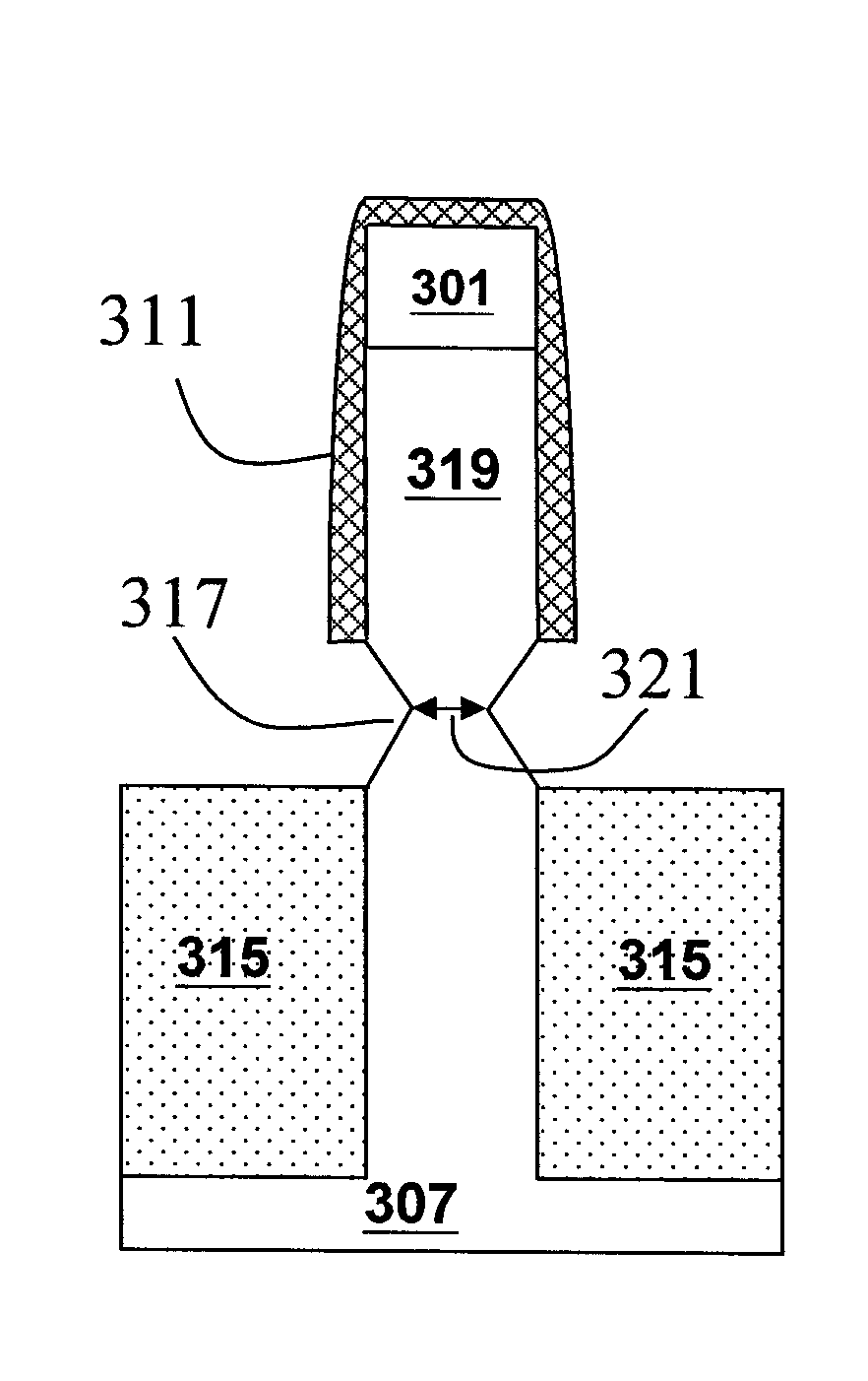
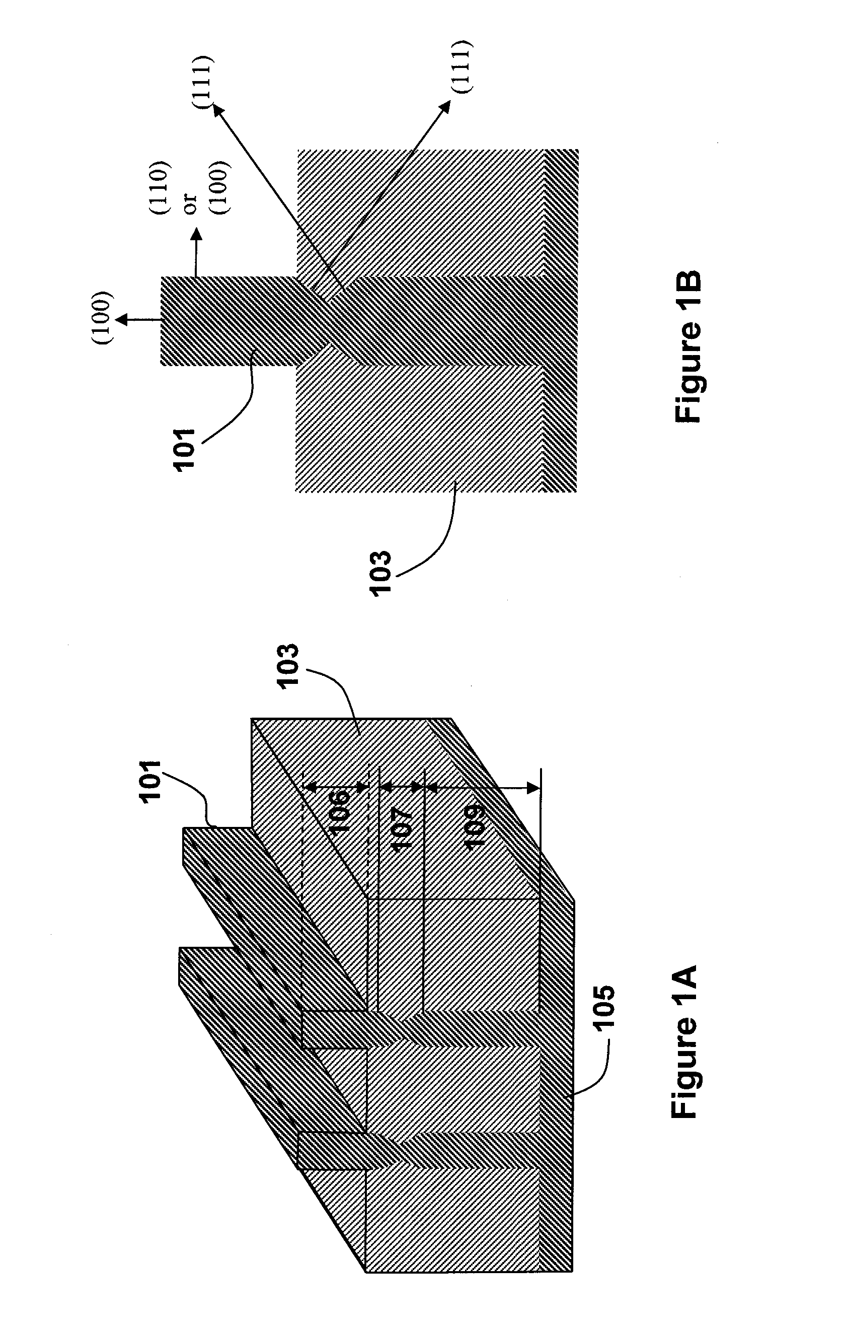
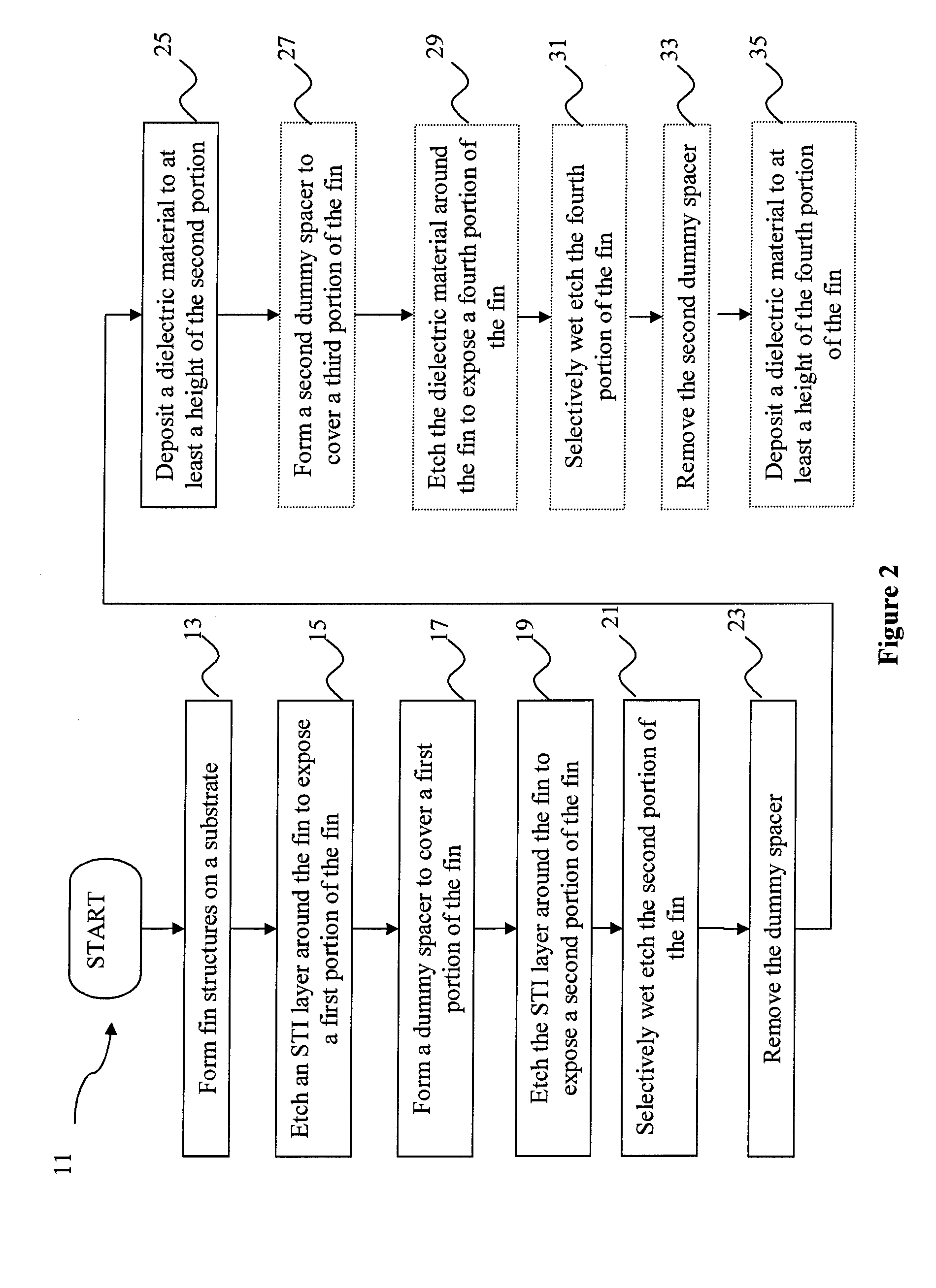
[0010]The making and using of illustrative embodiments are discussed in detail below. It should be appreciated, however, that the disclosure provides many applicable inventive concepts that can be embodied in a wide variety of specific contexts. Specific examples of components and arrangements are described below to simplify the present disclosure. These are, of course, merely examples and are not intended to be limiting. For example, the formation of a first feature over or on a second feature in the description that follows may include embodiments in which the first and second features are formed in direct contact, and may also include embodiments in which additional features may be formed between the first and second features, such that the first and second features may not be in direct contact. Of course, the description may specifically state whether the features are directly in contact with each other. In addition, the present disclosure may repeat reference numerals and / or le...


PUM


Abstract

A transistor includes a notched fin covered under a shallow trench isolation layer. One or more notch may be used, the size of which may vary along a lateral direction of the fin. In some embodiments, The notch is formed using anisotropic wet etching that is selective according to silicon orientation. Example wet etchants are tetramethylammonium hydroxide (TMAH) or potassium hydroxide (KOH).

Description

TECHNICAL FIELD[0001]The disclosure relates generally to integrated circuit devices, and more particularly to structure and methods for forming fin field-effect transistors (FinFETs).BACKGROUND[0002]In the rapidly advancing semiconductor manufacturing industry, complementary metal oxide semiconductor (CMOS) FinFET devices may be used in many logic and other applications and are integrated into various different types of semiconductor devices. FinFET devices typically include semiconductor fins with high aspect ratios in which the channel and source / drain regions for the transistor are formed. A gate is formed over and along the sides of a portion of the semiconductor fins. The increased surface area of the channel and source / drain regions in a FinFET results in faster, more reliable and better-controlled semiconductor transistor devices.[0003]Current FinFET technology, however, has challenges. For example, the channel is usually formed from the bulk substrate and is susceptible to a...

Claims


Application Information

Patent Timeline
Patent Type & Authority Applications(United States)
IPC IPC(8): H01L29/78H01L21/76
CPCH01L29/66795H01L29/7853H01L29/7851
Inventor TSENG, CHIH-HUNGLIN, DA-WENCHAN, CHIEN-TAILIN, CHIA-PINWENG, LI-WENCHANG, AN-SHENWU, CHUNG-CHENG
Owner TAIWAN SEMICON MFG CO LTD
Why Eureka
Try Eureka