Wafer processing tape, method of manufacturing wafer processing tape, and method of manufacturing semiconductor device

a technology of wafer processing tape and wafer ring, which is applied in the direction of film/foil adhesive, transportation and packaging, paper/cardboard containers, etc., can solve the problems of affecting the implementation of processes, requiring a greater peeling force to peel off the inner portion, etc., so as to ensure the peeling strength between the wafer processing tape and the wafer ring, the effect of improving workability and ensuring the fabrication yield of the semiconductor devi

Active Publication Date: 2012-04-19
RESONAC CORP
View PDF3 Cites 4 Cited by
  • Summary
  • Abstract
  • Description
  • Claims
  • Application Information

AI Technical Summary

Benefits of technology

[0022]According to this method of manufacturing a semiconductor device, since a peeling strength between the wafer processing tape and the wafer ring can be sufficiently ensured, the wafer processing tape can be suppressed from becoming peeled off from the wafer ring during processes. Therefore, workability can be improved and a fabrication yield of the semiconductor device can be ensured.
[0023]According to the present invention, a peeling strength with a wafer ring can be improved. In addition, a fabrication yield of the semiconductor device can be ensured.

Problems solved by technology

At this point, if the peeling strength between the wafer processing tape and the wafer ring is insufficient, the wafer processing tape peels off from the wafer ring during respective processes such as the dicing process and the die bonding process, and may adversely affect implementation of the processes.
However, due to an increase in a peeled area and the fact that a point of the pulling action is positioned further inward from the inner portion, a greater peeling force is required to peel off the inner portion.

Method used


Image

  • Wafer processing tape, method of manufacturing wafer processing tape, and method of manufacturing semiconductor device
  • Wafer processing tape, method of manufacturing wafer processing tape, and method of manufacturing semiconductor device
  • Wafer processing tape, method of manufacturing wafer processing tape, and method of manufacturing semiconductor device

Examples


Embodiment Construction

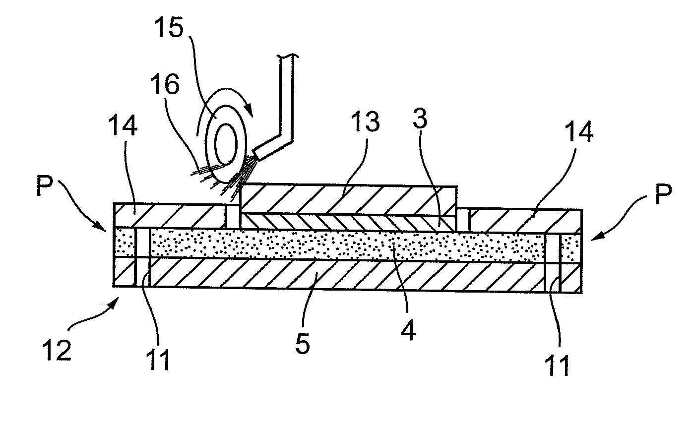
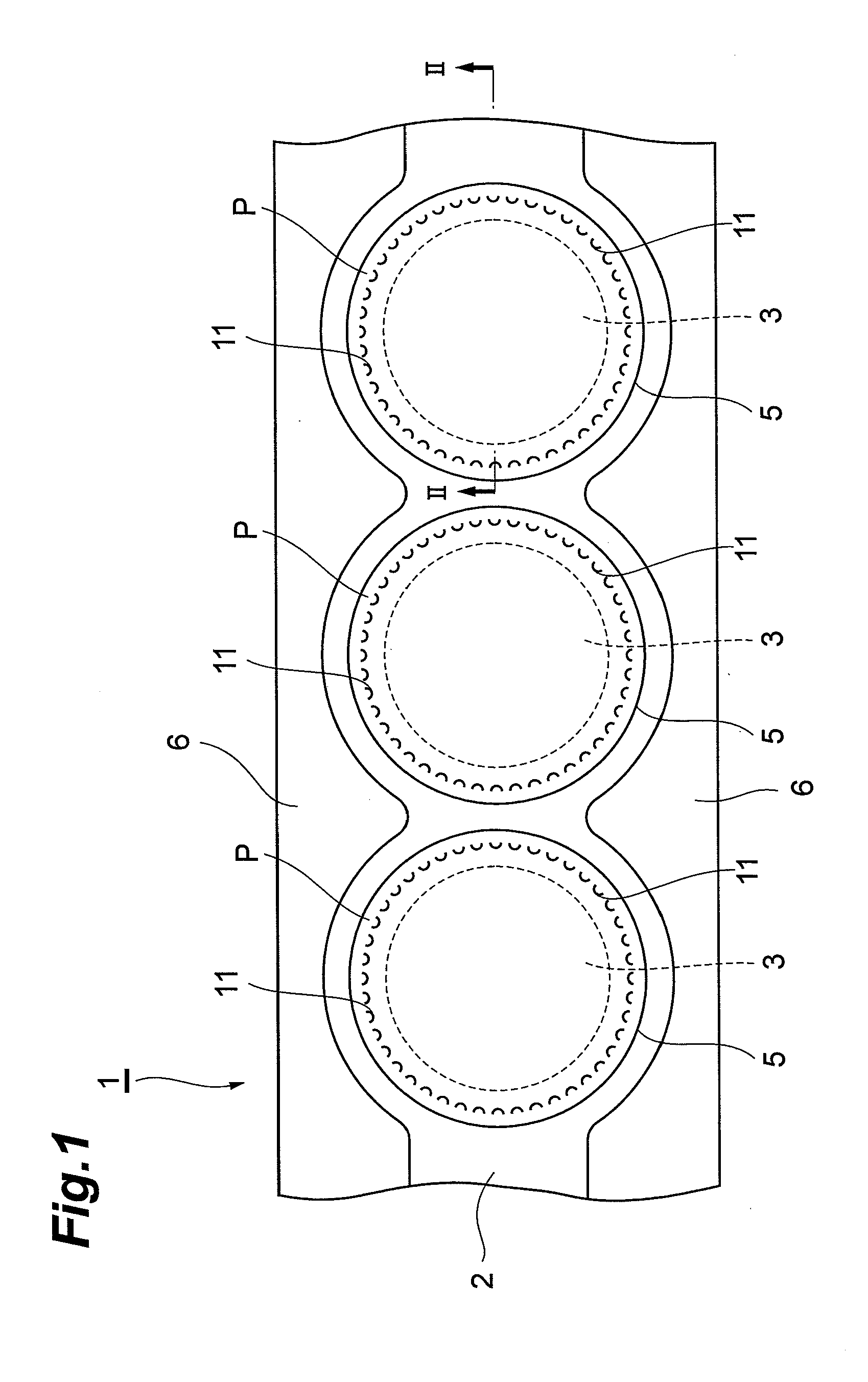
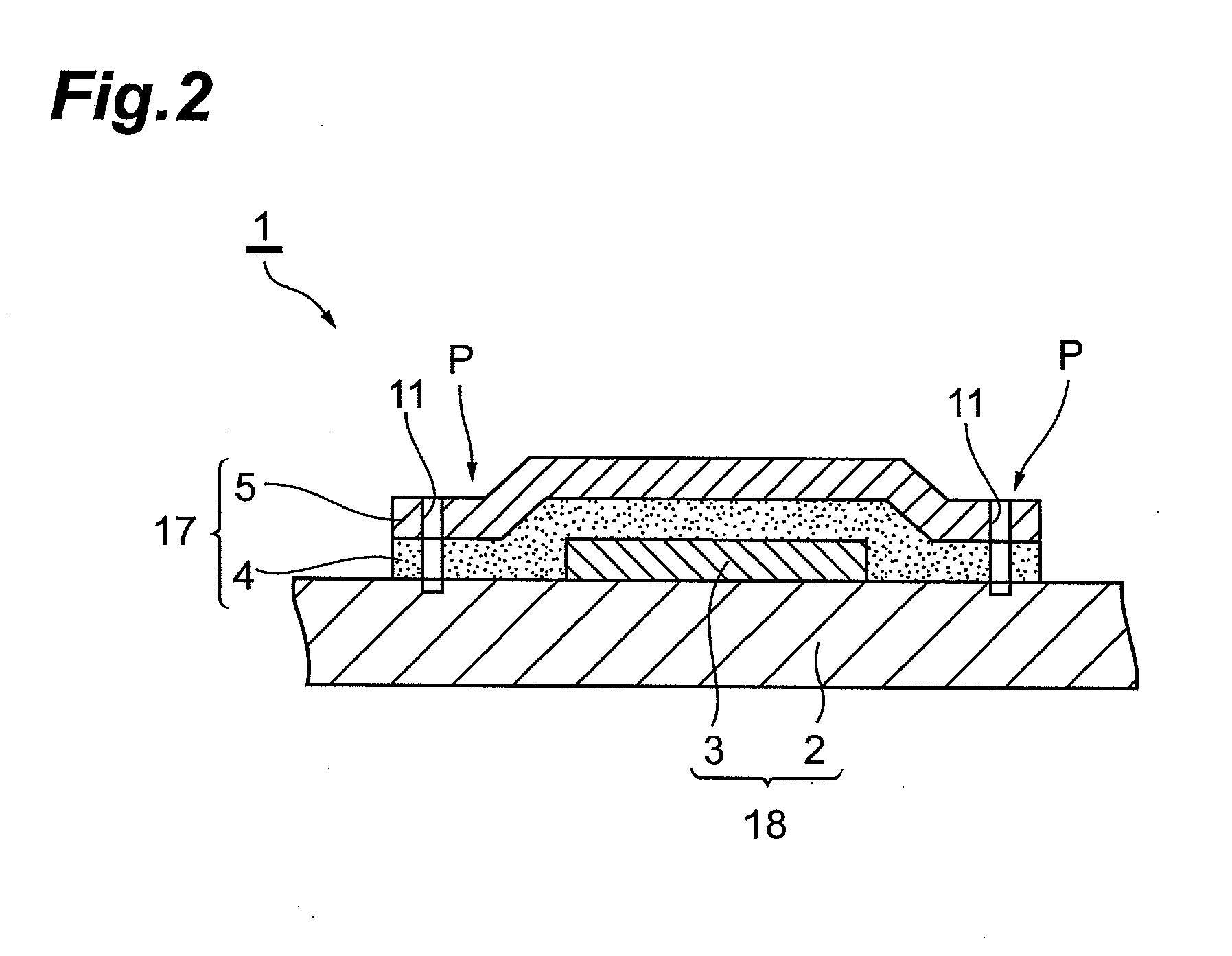
[0040]Hereinafter, preferred embodiments of a wafer processing tape, a method of manufacturing the wafer processing tape, and a method of manufacturing a semiconductor device using the wafer processing tape according to the present invention will be described in detail with reference to the drawings.

[0041][Configuration of Wafer Processing Tape]

[0042]FIG. 1 is a plan view showing an embodiment of a wafer processing tape according to the present invention. In addition, FIG. 2 is a cross-sectional view taken along II-II in FIG. 1. A wafer processing tape 1 in FIGS. 1 and 2 is a long tape used for dicing of a semiconductor wafer and for die bonding of a semiconductor chip obtained by dicing, and is normally wound into a roll.

[0043]As shown in FIGS. 1 and 2, the wafer processing tape 1 has been precut and comprises: a release base material 2 that constitutes a base of the tape; an adhesive layer 3 circularly provided at regular intervals on one surface of the release base material 2 so ...


PUM

PropertyMeasurementUnit
diameteraaaaaaaaaa
diameteraaaaaaaaaa
diameteraaaaaaaaaa

Abstract

In a wafer processing tape, circular or tongue-shaped notched parts facing the center of an adhesive layer, as seen in a plan view, are formed so as to correspond to a pasting region to a wafer ring to a depth that reaches a release base material from the side of a base material film. Due to the formation of the notched parts, when a peeling force acts on the wafer processing tape, portions of a tacky material layer and the base material film which are more outward than the notched parts are peeled off first, and a portion that is more inward than the notched parts remains on the wafer ring in a protruding state. Accordingly, a peeling strength between the wafer processing tape and the wafer ring can be increased. Methods of manufacturing the tape and a semiconductor device are also provided.

Description

CROSS-REFERENCE TO RELATED APPLICATION[0001]This application claims priority to Provisional Application No. 61 / 446,987 filed on Feb. 25, 2011 by the same Applicant, which is hereby incorporated by reference in its entirety.BACKGROUND OF THE INVENTION[0002]1. Field of the Invention[0003]The present invention relates to a wafer processing tape used for dicing of a semiconductor wafer and for die bonding of a semiconductor chip obtained by dicing or the like, a method of manufacturing the wafer processing tape, and a method of manufacturing a semiconductor device using the wafer processing tape.[0004]2. Related Background Art[0005]In recent years, there has been a rapid increase in demands for a wider range of functions, lighter weight, and smaller sizes in mobile-related devices. Accordingly, there has been a stronger need for high-density packaging of semiconductor chips. In particular, development has been focused on stacked multi-chip packages in which semiconductor chips are lamin...

Claims


Application Information

Patent Timeline
Patent Type & Authority Applications(United States)
IPC IPC(8): H01L21/78B32B37/14B32B33/00B32B37/12C09J7/20
CPCH01L21/568H01L21/67132H01L23/3135H01L21/6836H01L21/78Y10T156/1052H01L2924/0002Y10T428/1476Y10T156/10H01L2924/00C09J2203/326C09J7/20C09J7/403C09J2301/18C09J2301/204C09J2301/208C09J2301/122C09J2301/302C09J7/22C09J7/30C09J7/38H01L23/293H01L2221/68327
Inventor TANIGUCHI, KOUHEIMATSUZAKI, TAKAYUKIKATOU, SHINYAKOMORIDA, KOUJIMASHINO, MICHIOSAKUTA, TATSUYAKATOU, RIE
Owner RESONAC CORP
Why Eureka
Try Eureka