Strain compensated short-period superlattices on semipolar or nonpolar GAN for defect reduction and stress engineering

Inactive Publication Date: 2012-05-03
RGT UNIV OF CALIFORNIA
View PDF0 Cites 38 Cited by
  • Summary
  • Abstract
  • Description
  • Claims
  • Application Information

AI Technical Summary

Benefits of technology

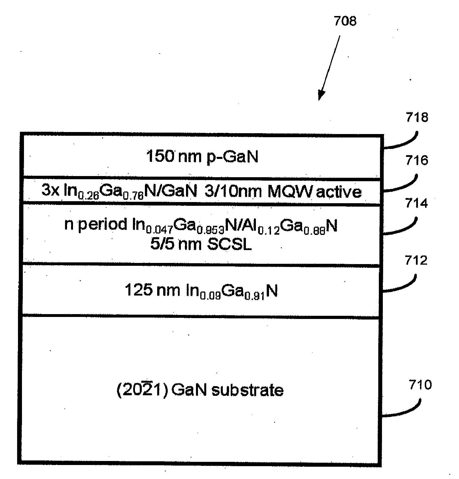
[0019]The present invention further discloses a method of fabricating a (AlInGaN) based semiconductor device, comprising growing a first layer that is a semipolar or nonpolar III-nitride (AlInGaN) layer having a lattice constant that is partially or fully relaxed, deposited on a substrate or a template, wherein there are one or more dislocations at a heteroi

Problems solved by technology

However, threshold current densities (Jth) are still high relative to shorter wavelength devices, and output power is limited to 50 mW.
Aside from phase segregation, one of the most significant challenges in growing the active regions for long wavelength devices is managing the strain for active regions with Indium

Method used


Image

  • Strain compensated short-period superlattices on semipolar or nonpolar GAN for defect reduction and stress engineering
  • Strain compensated short-period superlattices on semipolar or nonpolar GAN for defect reduction and stress engineering
  • Strain compensated short-period superlattices on semipolar or nonpolar GAN for defect reduction and stress engineering

Examples


Embodiment Construction

[0031]In the following description of the preferred embodiment, reference is made to the accompanying drawings which form a part hereof, and in which is shown by way of illustration a specific embodiment in which the invention may be practiced. It is to be understood that other embodiments may be utilized and structural changes may be made without departing from the scope of the present invention.

[0032]Nomenclature

[0033]GaN and its ternary and quaternary compounds incorporating aluminum and indium (AlGaN, InGaN, AlInGaN) are commonly referred to using the terms (Al,Ga,In)N, III-nitride, Group III-nitride, nitride, Al(1-x-y)InyGaxN where 0


PUM


Abstract

An (AlInGaN) based semiconductor device, comprising a first layer that is a semipolar or nonpolar nitride (AlInGaN) layer having a lattice constant that is partially or fully relaxed, deposited on a substrate or a template, wherein there are one or more dislocations at a heterointerface between the first layer and the substrate or the template; one or more strain compensated layers on the first layer, for defect reduction and stress engineering in the device, that is lattice matched to a larger lattice constant of the first layer; and one or more nonpolar or semipolar (AlInGaN) device layers on the strain compensated layers.

Description

CROSS REFERENCE TO RELATED APPLICATIONS[0001]This application claims the benefit under 35 U.S.C. Section 119(e) of co-pending and commonly-assigned U.S. Provisional Application Ser. No. 61 / 408,280 filed on Oct. 29, 2010, by Matthew T. Hardy, Steven P. DenBaars, James S. Speck, and Shuji Nakamura, entitled “STRAIN COMPENSATED SHORT-PERIOD SUPERLATTICES ON SEMIPOLAR GAN FOR DEFECT REDUCTION AND STRESS ENGINEERING,” attorney's docket number 30794.396-US-P1 (2011-203), which application is incorporated by reference herein.[0002]This application is related to the following co-pending and commonly-assigned U.S. patent applications:[0003]U.S. Utility application Ser. No. 12 / 661,652, filed on Aug. 23, 2010, by Hiroaki Ohta et. al., entitled “ANISOTROPIC STRAIN CONTROL IN SEMIPOLAR NITRIDE QUANTUM WELLS BY PARTIALLY OR FULLY RELAXED ALUMINUM INDIUM GALLIUM NITRIDE LAYERS WITH MISFIT DISLOCATIONS,” attorney's docket number 30794.318-US-U1 (2009-743-2), which application claims the benefit und...

Claims


Application Information

Patent Timeline
IPC IPC(8): H01L29/15H01L21/20
CPCH01L21/02389H01L21/0242H01L21/02433H01L21/02458H01L21/02507H01L21/0254B82Y20/00H01L33/0075H01L33/16H01L33/32H01S5/3201H01S5/3216H01S5/34333H01L21/0262
Inventor HARDY, MATTHEW T.DENBAARS, STEVEN P.SPECK, JAMES S.NAKAMURA, SHUJI
Owner RGT UNIV OF CALIFORNIA
Why Eureka
Try Eureka