Analog signal processor for nonlinear predistortion of radio-frequency signals
- Summary
- Abstract
- Description
- Claims
- Application Information
AI Technical Summary
Benefits of technology
Problems solved by technology
Method used
Image

Examples
first embodiment
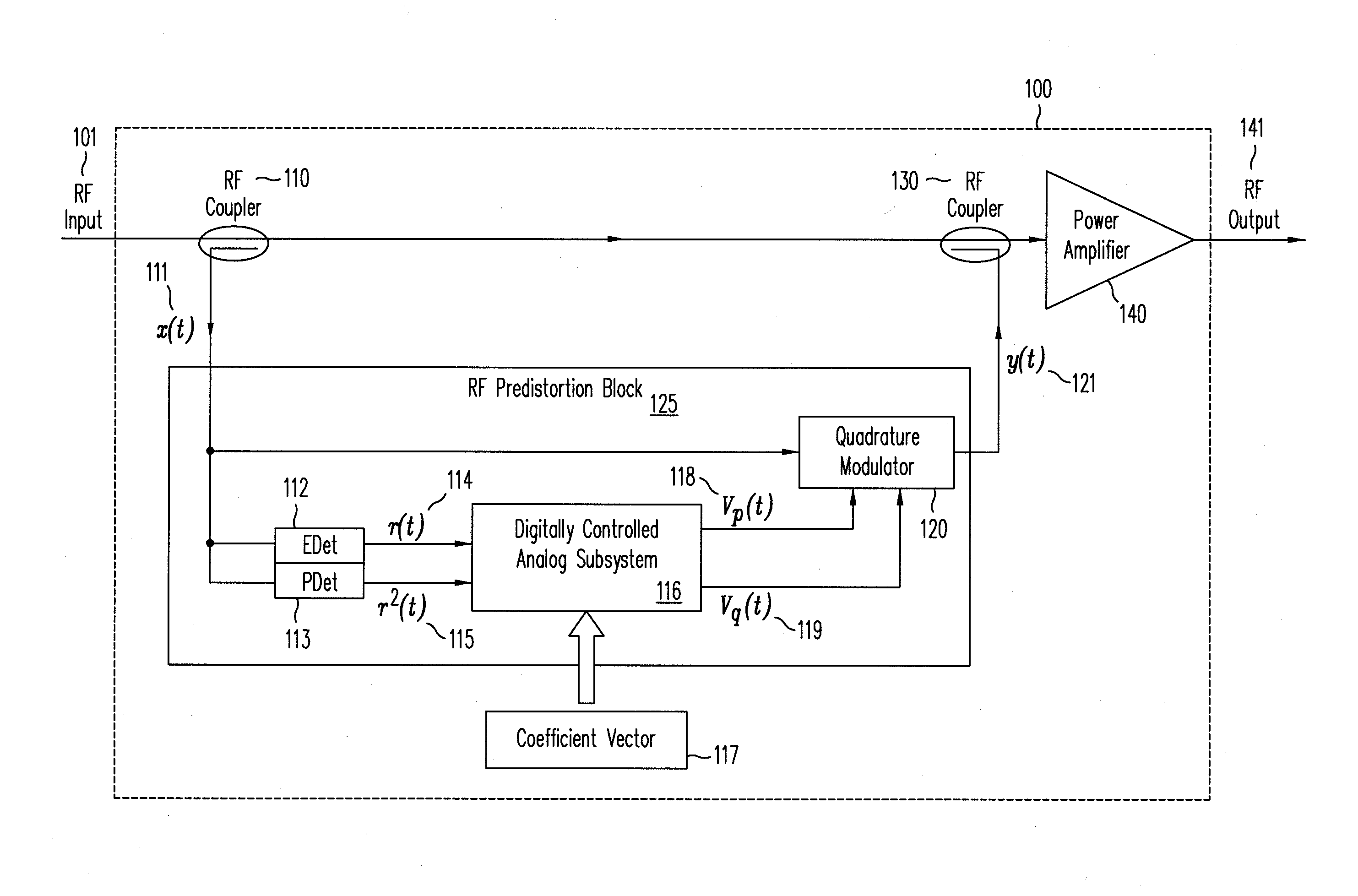
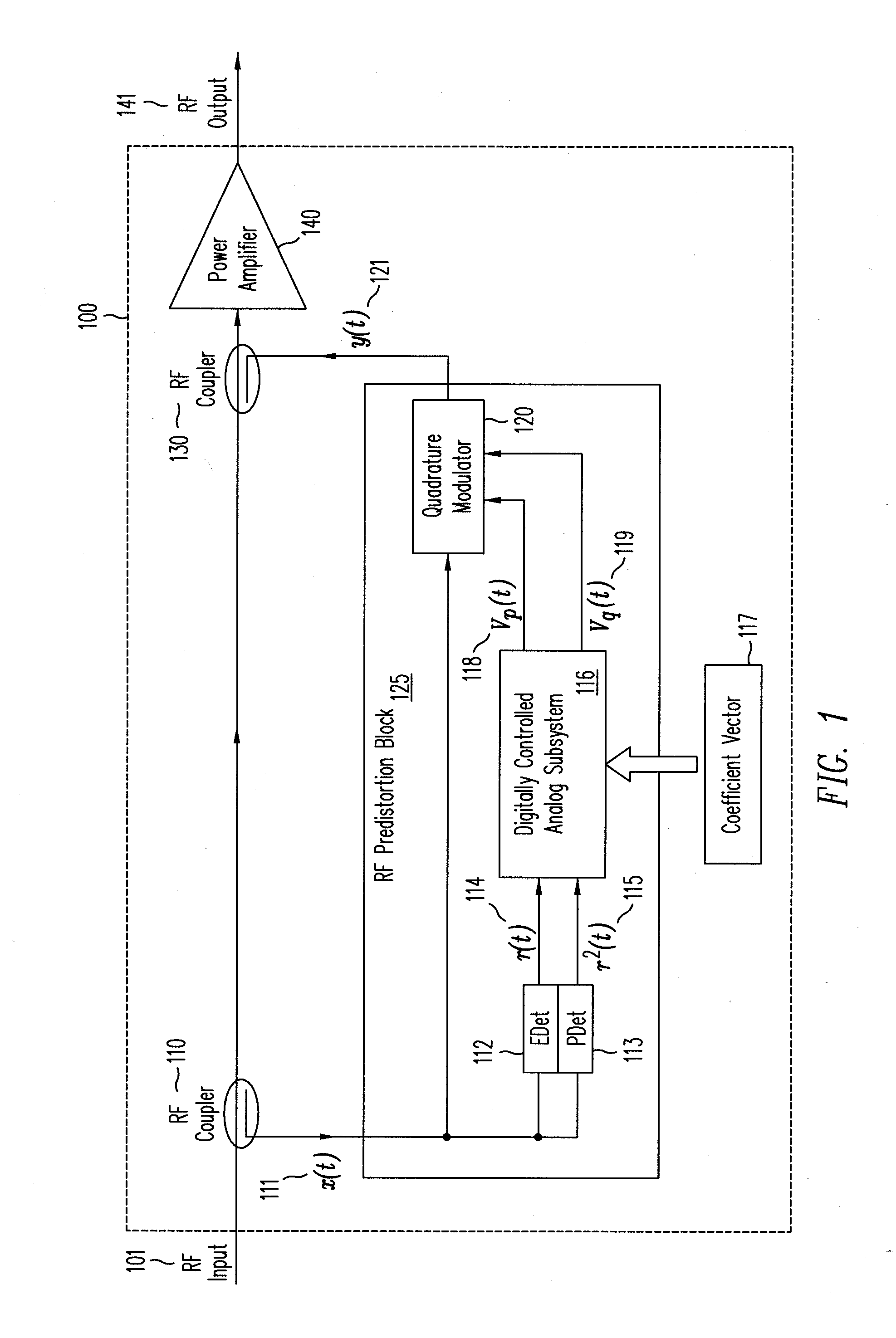
[0026]In a linear power amplifier, a linear PA circuit 100 is shown in FIG. 1. At RF Input signal 101 is injected into the circuit. An RF coupler 110 provides incoming RF input signal 101 to RF predistortion block 125. For illustrative purpose, RF input signal 101 may be a time-varying signal, expressed as x(t) 111, which may have the form shown in Equ. 1, where r(t) is the envelope of the signal.
x(t)=r(t)cos [2πf+φ(t)] Equ. 1
[0027]RF distribution block 125 comprises envelop detector (EDet) 112, power detector (PDet) 113, digitally controlled analog subsystem (DCAS) 116 and quadrature modulator 120. RF predistortion block 125 may be constructed as a single integrated circuit or as multiple integrated circuits or by discrete components, as desired.
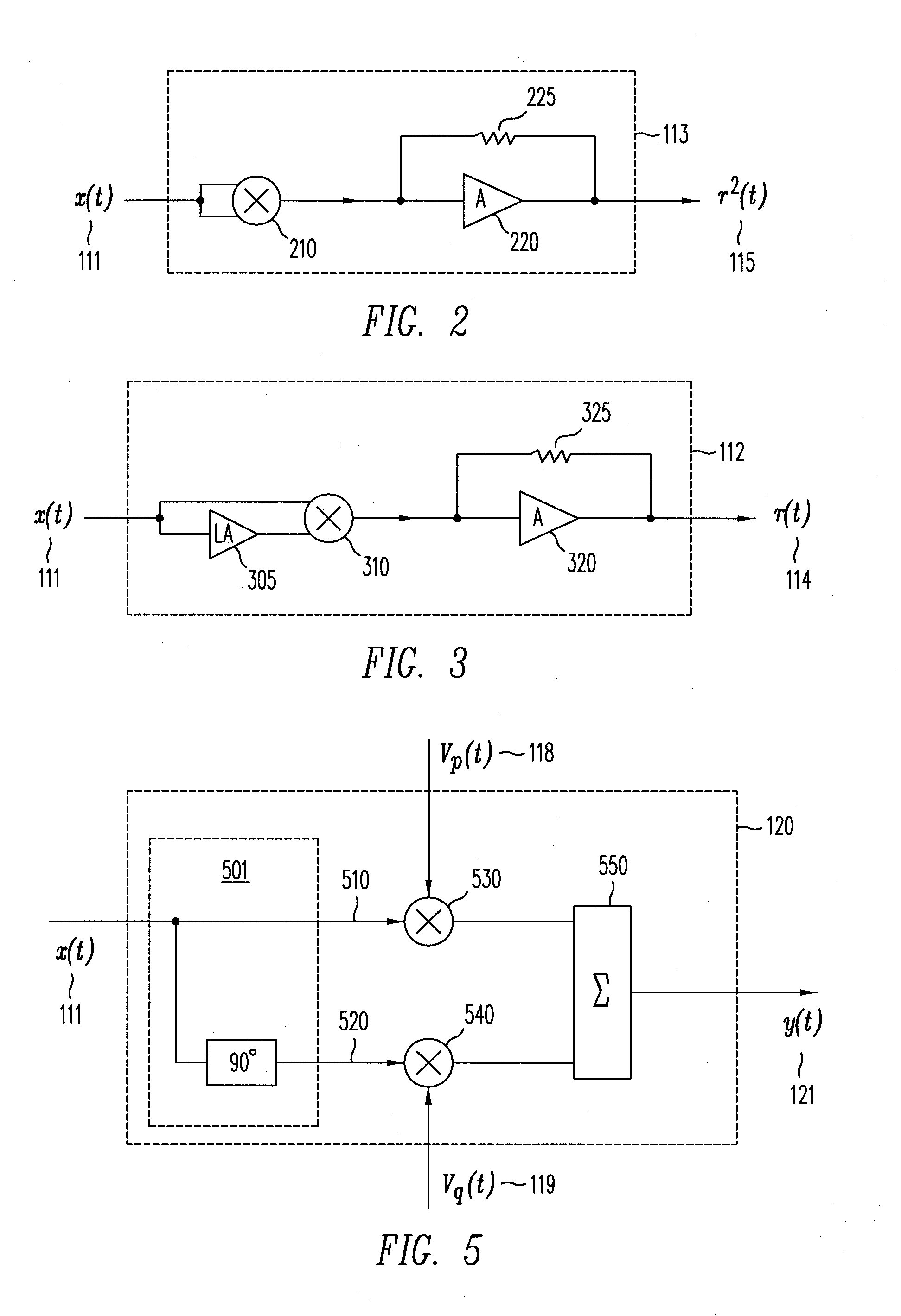
[0028]The envelope r(t) of x(t) 111, is output by envelop detector 112 as r(t) 114. The power of x(t) 111 is output by power detector 113 as r2(t) 115. The envelop and power of x(t) 111, r(t) 114 and r2(t) 115, respectively, are input to D...
second embodiment
[0043]In a linear power amplifier, a linear PA 800 is shown in FIG. 8. In addition to the components of linear PA 100 of FIG. 4, linear PA 800 further comprises RF delay elements RFD1 810 and RFD2 820, where each delay is typically between 5 ns to 15 ns. If the RF predistortion block 125 is implemented as an integrated circuit, the memory compensation capability can be significantly improved by using off-chip RF delay elements RFD1 810 and RFD2 820 in the form of transmission lines. In one embodiment, RFD1 810 and RFD2 820 can each provide suitable transmission delays (e.g., 4 ns), such that the delayed terms in RF predistortion block 125 may provide non-causal (i.e., negative valued, relative the delays of RFD1) predistortion terms.
third embodiment
[0044]In a linear power amplifier, a linear PA 900 is shown in FIG. 9. Linear PA 900 employs at least three RF predistortion blocks 125a, 125b and 125c connected in parallel, as described in reference to FIG. 1. RF predistortion blocks 125a, 125b and 125c may all reside on a single chip integrated circuit 980. Linear PA 900 further comprises a combiner 970 connected to RF predistortion blocks 125a, 125b and 125c that sums together the signals emanating from the quadrature modulators in each block. Linear PA 900 further comprises RF delay elements 910, 920 and 930. RF delay elements 910, 920 and 930 delay the RF input 101 differently for each RF predistortion block 125a, 125b and 125c. Without limiting its application to other PA architectures, linear power amplifier 900 is suitable for high power Doherty amplifiers. Linear Amplifier 900, and variations based on the same principle, provides many options to fine tune the required predistortion to achieve a desired linear output profil...
PUM
 Abstract
Description
Claims
Application Information