
Method to reduce ground-plane poisoning of extremely-thin soi (ETSOI) layer with thin buried oxide

a technology of buried oxide and buried soi, applied in the field of ultrathinbody and box, can solve the problems of short channel effect (sce), increased vt variability, and short punch-through device, and achieve the effect of slowing down the rate of dopant diffusion

Active Publication Date: 2012-05-10
GLOBALFOUNDRIES US INC
View PDF5 Cites 14 Cited by
  • Summary
  • Abstract
  • Description
  • Claims
  • Application Information

AI Technical Summary

Benefits of technology

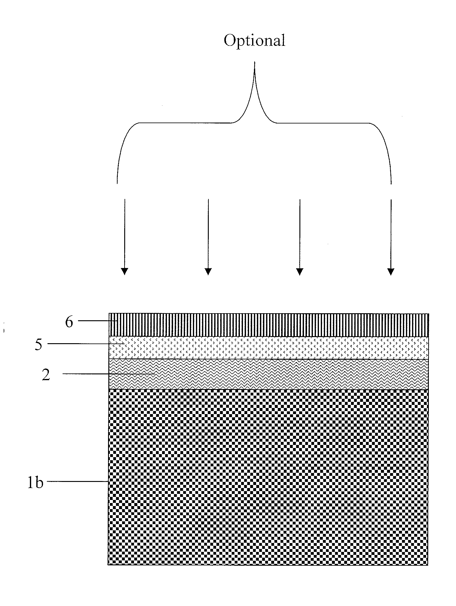
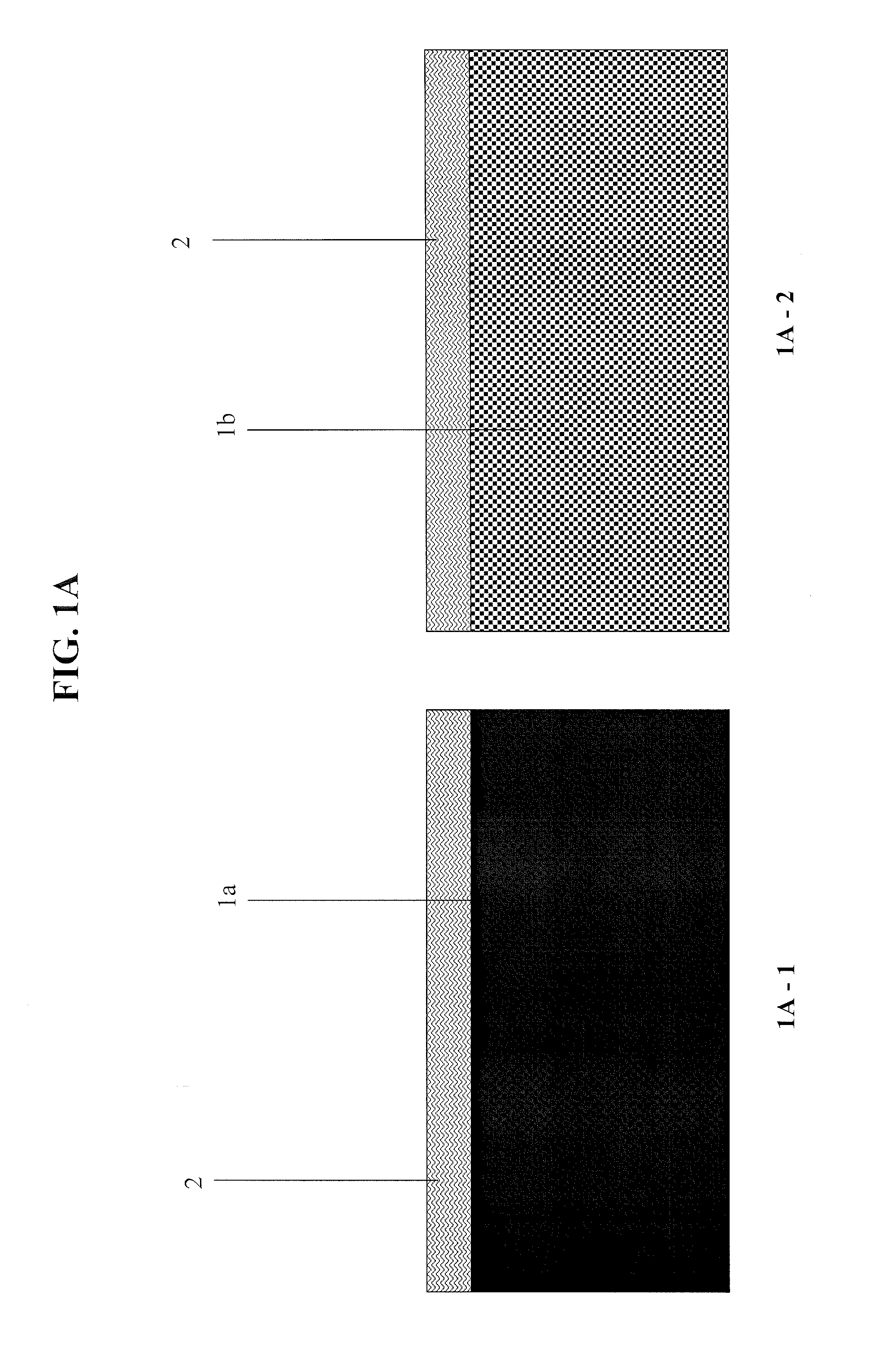
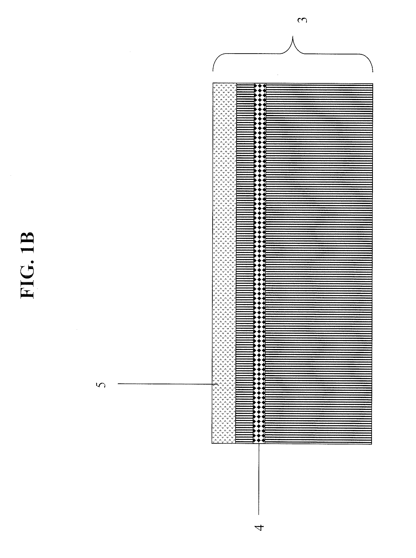
[0004]The present disclosure therefore provides for ultra-thin-body-and-BOX and Double BOX fully depleted SOI devices having an epitaxial diffusion-retarding semiconductor layer, as well as methods of making these devices. The epitaxial diffusion-retarding semiconductor layer, which is crystalline in nature, slows the rate of dopant diffusion from the substrate into the SOI channel. The dopant concentration in the SOI channel of devices of the present disclosure, which comprise an epitaxial diffusion-retarding semiconductor layer, are approximately 50 times less than the dopant concentration in SOI channels of devices without the epitaxial diffusion-retarding semiconductor layer.

Problems solved by technology

One problem associated with CMOS scaling involves short channel effects (SCE's).
This is problematic because the dopant concentration in the thin SOI channel after ion implantation may be ˜5-8e17 / cm3, and could lead to increased Vt variability due to random-dopant fluctuations.
However, experiments on such predoped UTBB substrates have shown that the dopant diffuses from the substrate through the thin-BOX and into the SOI channel when exposed to the FEOL thermal budget resulting in punch-through (shorted) devices.

Method used


Image

  • Method to reduce ground-plane poisoning of extremely-thin soi (ETSOI) layer with thin buried oxide
  • Method to reduce ground-plane poisoning of extremely-thin soi (ETSOI) layer with thin buried oxide
  • Method to reduce ground-plane poisoning of extremely-thin soi (ETSOI) layer with thin buried oxide

Examples


example 1

[0046]TCAD simulations on ultra-thin-body-and-BOX devices of the present disclosure were performed. The devices comprised an in-situ doped substrate having an Si:C epitaxial diffusion-retarding semiconductor layer between a thin oxide layer and GP layer. The simulations account for the entire FEOL thermal budget, and show the boron concentration at the end of the process for devices with an Si:C layer and devices without an Si:C layer. In particular, the simulations showed that the devices having a sufficiently thick (10-30 nanometers) Si:C layer with 1% C epitaxial film inserted between the Si substrate and the GP layer slowed boron diffusion into the SOI channel approximately 50 times better than the devices without the Si:C layer after exposure to FEOL thermal budget.


PUM


Abstract

The present disclosure, which is directed to ultra-thin-body-and-BOX and Double BOX fully depleted SOI devices having an epitaxial diffusion-retarding semiconductor layer that slows dopant diffusion into the SOI channel, and a method of making these devices. Dopant concentrations in the SOI channels of the devices of the present disclosure having an epitaxial diffusion-retarding semiconductor layer between the substrate and SOI channel are approximately 50 times less than the dopant concentrations measured in SOI channels of devices without the epitaxial diffusion-retarding semiconductor layer.

Description

TECHNICAL FIELD[0001]The present disclosure relates to ultra-thin-body-and-BOX (“UTBB”) and Double BOX fully depleted SOI devices having an epitaxial diffusion-retarding semiconductor layer between the substrate and buried oxide layers, as well as to a method of making these devices. The epitaxial diffusion-retarding semiconductor layer of these devices, which is crystalline in nature, slows the rate of dopant diffusion from the substrate into the SOI channel. More generally, the present disclosure relates to a method of reducing dopant diffusion into the SOI channel of an SOI device after front-end-of-line (FEOL) thermal budget processing.BACKGROUND OF THE DISCLOSURE[0002]To meet the increasing demands for smaller electronic devices, CMOS devices have continuously been scaled down. One problem associated with CMOS scaling involves short channel effects (SCE's). Ultra-thin-body-and-BOX (i.e., UTBB, UT2B, or UTB2) fully depleted SOI devices are an attractive candidate for further CMO...

Claims


Application Information

Patent Timeline
Patent Type & Authority Applications(United States)
IPC IPC(8): H01L27/12H01L21/762H01L29/24
CPCH01L29/78603H01L21/76254
Inventor CHENG, KANGGUODORIS, BRUCE B.KHAKIFIROOZ, ALIKULKARNI, PRANITASHAHIDI, GHAVAM G.
Owner GLOBALFOUNDRIES US INC
Learn More