Input/output device and driving method thereof

a technology of input/output device and driving method, which is applied in the direction of instruments, television systems, material analysis, etc., can solve the problems of insufficient reduce the quality of input/output image, and increase the switching speed of input/output image, reduce the quality of input/output image, and reduce the effect of flicker in input/output imag

Active Publication Date: 2012-05-17
SEMICON ENERGY LAB CO LTD
View PDF2 Cites 2 Cited by
  • Summary
  • Abstract
  • Description
  • Claims
  • Application Information

AI Technical Summary

Benefits of technology

[0017]The above-described structure reduces the adverse effect of light around the input/output device on the generated optical data.
[0018]One embodiment of the present invention increases the switching

Problems solved by technology

A conventional input/output device like that shown in Patent Document 1 has a problem of the insufficient quality of a displayed image.
Consequently, every time display data in the plurality of light emission circuits are refreshed to ma

Method used


Image

  • Input/output device and driving method thereof
  • Input/output device and driving method thereof
  • Input/output device and driving method thereof

Examples


embodiment 1

[0029]In this embodiment, an example of an input / output device that can output data by displaying an image and can input data by using incident light is described.

[0030]An example of the input / output device in this embodiment will be described with reference to FIGS. 1A and 1B.

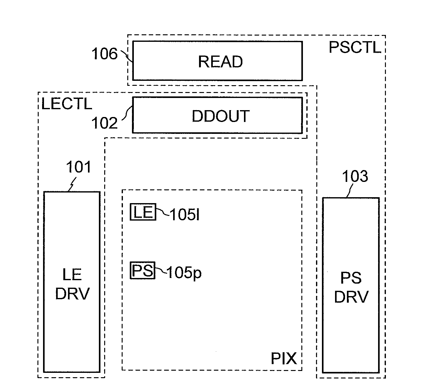
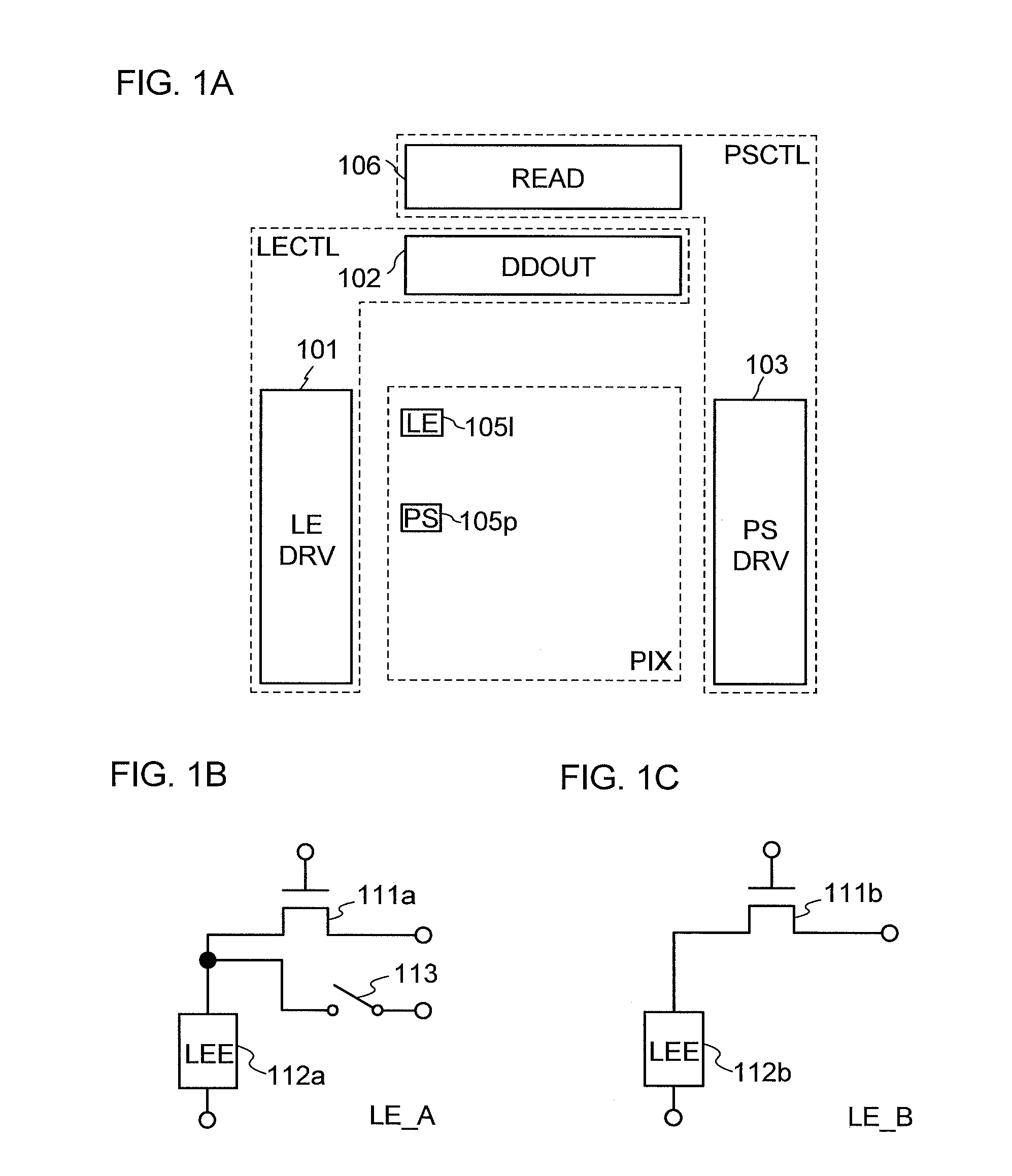
[0031]First, the structural example of the input / output device of this embodiment will be described with reference to FIG. 1A. FIG. 1A is a schematic diagram illustrating the structural example of the input / output device in this embodiment.

[0032]The input / output device in FIG. 1A includes a light emission controller LECTL, a photodetection controller PSCTL, and a pixel area PIX.

[0033]The light emission controller LECTL is a part controlling light emitting operation in the input / output device.

[0034]The photodetection controller PSCTL is a part controlling photodetection operation in the input / output device.

[0035]The pixel area PIX is a part inputting and outputting data by performing the light emitting operatio...

embodiment 2

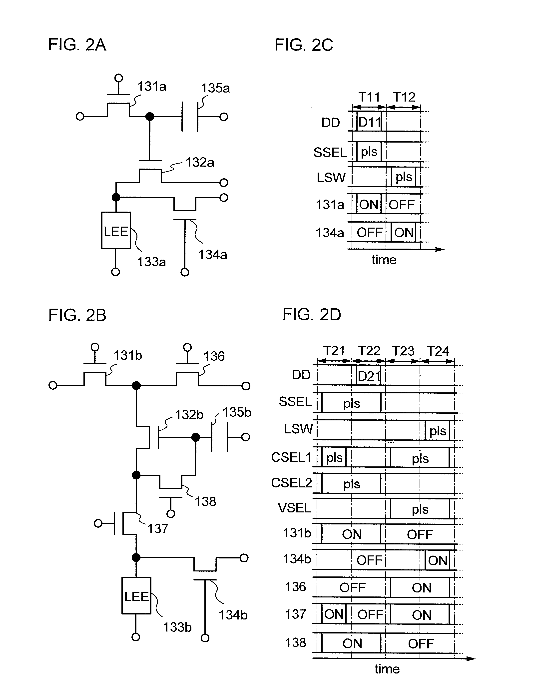
[0116]In this embodiment, examples of the light emission circuit in one example of the input / output device of Embodiment 1 are described.

[0117]Examples of the light emission circuit in this embodiment will be described with reference to FIGS. 2A to 2D.

[0118]First, examples of the configuration of the light emission circuit in this embodiment will be described with reference to FIGS. 2A and 2B. FIGS. 2A and 2B illustrate examples of the configuration of the light emission circuit in this embodiment.

[0119]The light emission circuit in FIG. 2A includes a transistor 131a, a transistor 132a, a light emitting element (also called an LEE) 133a, a transistor 134a, and a capacitor 135a.

[0120]In the light emission circuit in FIG. 2A, the transistors 131a, 132a, and 134a are field-effect transistors.

[0121]Note that, in the input / output device, a capacitor includes a first capacitor electrode, a second capacitor electrode, and a dielectric layer overlapping with the first capacitor electrode a...

embodiment 3

[0174]In this embodiment, examples of the photodetection circuit in the input / output device of the above embodiment are described.

[0175]Examples of the photodetection circuit in this embodiment will be described with reference to FIGS. 3A to 3F. FIGS. 3A to 3F illustrate the examples of the photodetection circuit of this embodiment.

[0176]First, examples of the configuration of the photodetection circuit of this embodiment will be described with reference to FIGS. 3A to 3C. FIGS. 3A to 3C illustrate the examples of the configuration of the photodetection circuit of this embodiment.

[0177]The photodetection circuit illustrated in FIG. 3A includes a photoelectric transducer (PCE) 151a, a transistor 152a, and a transistor 153a.

[0178]Note that in the photodetection circuit illustrated in FIG. 3A, the transistor 152a and the transistor 153a are field-effect transistors.

[0179]A photodetection reset signal (also called a signal PRST) is input to the first current terminal of the photoelectr...


PUM


Abstract

An input/output device includes a pixel area; a light emission circuit provided in the pixel area and configured to emit light; and a photodetection circuit provided in the pixel area and configured to generate a voltage having a value corresponding to an intensity of incident light. The light emission circuit includes a drive transistor and a light emitting element. The light emitting element includes a first current terminal electrically connected to the source or the drain of the drive transistor and a second current terminal to which a first voltage is input, and emits light in accordance with a current flowing between the first and second current terminals. The light emission circuit includes a switching element including a first terminal to which a second voltage is input, and a second terminal electrically connected to the first current terminal of the light emitting element.

Description

BACKGROUND OF THE INVENTION[0001]1. Field of the Invention[0002]An embodiment of the present invention relates to an input / output device and a driving method thereof.[0003]2. Description of the Related Art[0004]In recent years, technological development of a device having a function of outputting data and inputting data by using incident light (such a device is also called an input / output device) has been promoted.[0005]An example of the input / output device is an input / output device that includes a plurality of light emission circuits which serve as display circuits and a plurality of photodetection circuits (also called photosensors) arranged in the row and column directions and provided in a pixel area, and that has a function of detecting the coordinates of an object to be detected over the pixel area (also called a coordinate-detecting function) by detecting the intensity of light entering the photosensors and a function of generating the image data of the object (also called a ...

Claims


Application Information

Patent Timeline
IPC IPC(8): H01L31/16
CPCH01L27/14609H04N5/374H01L27/14665H04N25/76
Inventor KUROKAWA, YOSHIYUKIIKEDA, TAKAYUKI
Owner SEMICON ENERGY LAB CO LTD
Why Eureka
Try Eureka