Microelectronic package with terminals on dielectric mass
- Summary
- Abstract
- Description
- Claims
- Application Information
AI Technical Summary
Benefits of technology
Problems solved by technology
Method used
Image

Examples
Embodiment Construction
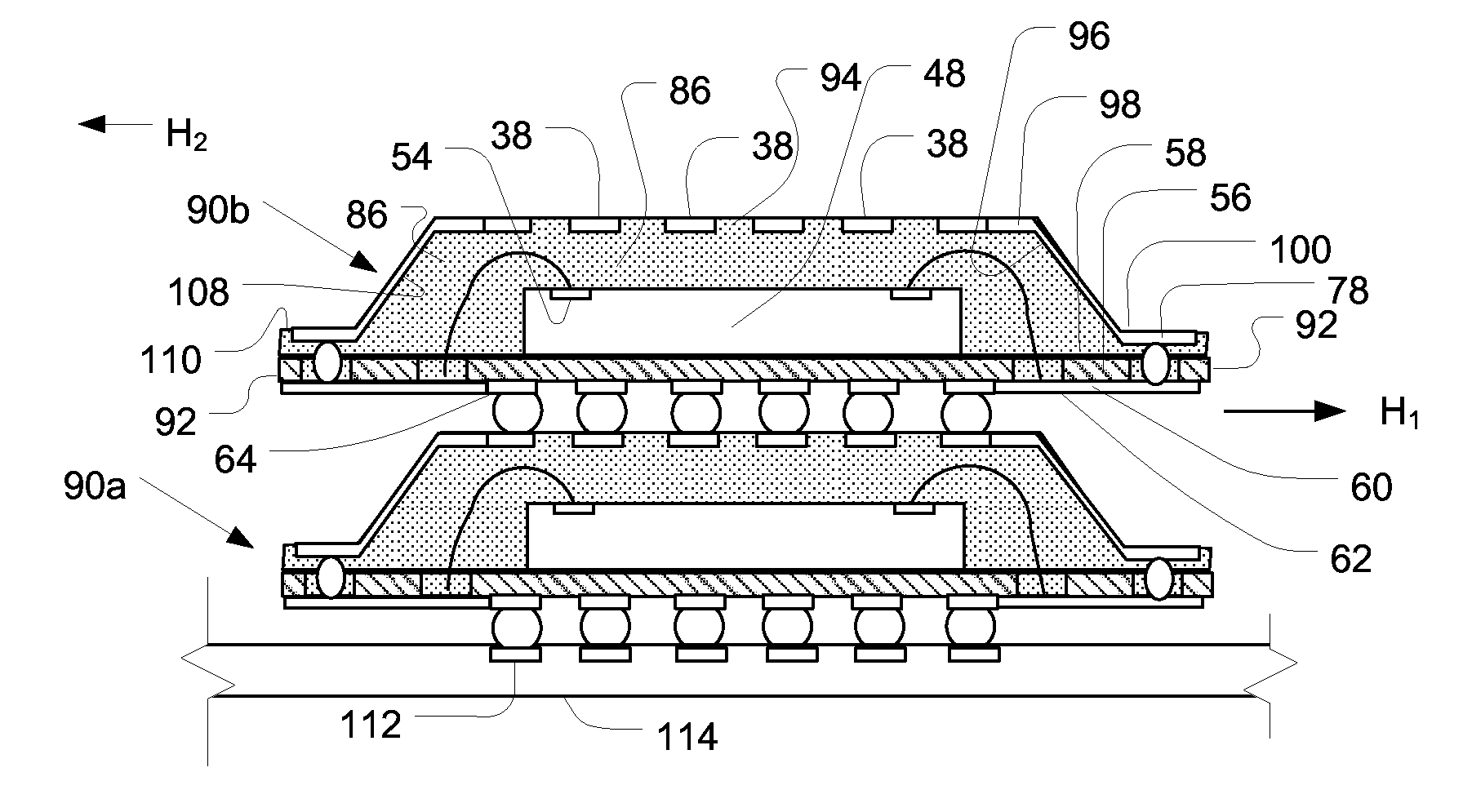
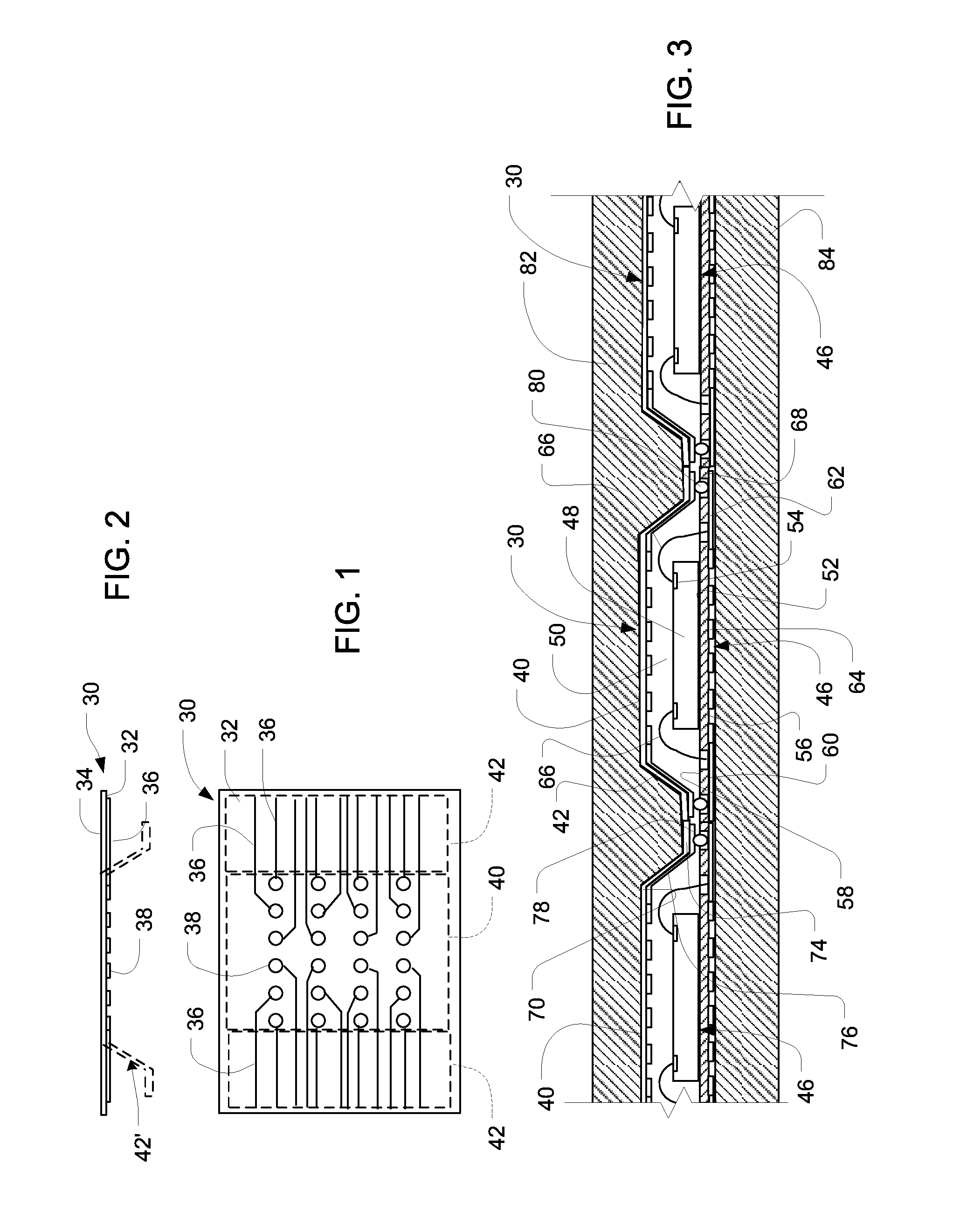
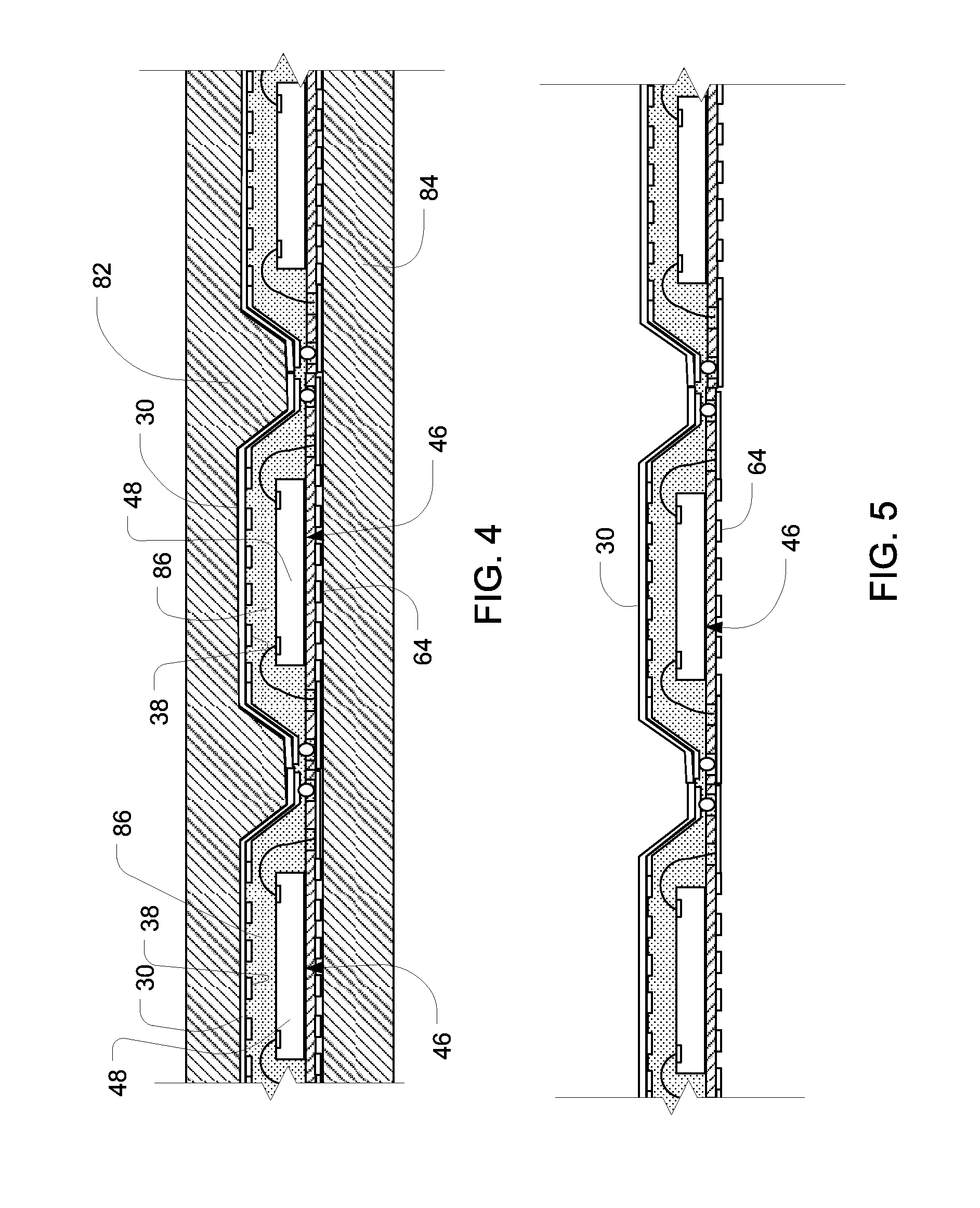
[0039]A component utilized in a manufacturing process according to one embodiment of the invention incorporates a carrier in the form of a metallic sheet 30 as, for example, a sheet of copper (FIGS. 1 and 2) having a first surface 32 and an opposite second surface 34. The first surface 32 bears a plurality of electrically conductive traces 36. The traces are formed as elongated strips of a conductive material, preferably a solid metal such as copper, gold, nickel, and combinations thereof on the first surface 32 of sheet 30. The traces are formed integrally with terminals 38 of similar composition. The terminals are disposed in a first portion 40 of the sheet, schematically indicated by a broken line. The traces extend from the terminals into a second portion 42. In this embodiment, second portion 42 includes regions on opposite sides of the first portion 40. Although only a few terminals 38 and a few traces 36 are depicted in FIGS. 1 and 2, in practice, there can be hundreds or mor...
PUM
 Abstract
Description
Claims
Application Information
 - Generate Ideas
- Intellectual Property
- Life Sciences
- Materials
- Tech Scout
- Unparalleled Data Quality
- Higher Quality Content
- 60% Fewer Hallucinations
Browse by: Latest US Patents, China's latest patents, Technical Efficacy Thesaurus, Application Domain, Technology Topic, Popular Technical Reports.
© 2025 PatSnap. All rights reserved.Legal|Privacy policy|Modern Slavery Act Transparency Statement|Sitemap|About US| Contact US: help@patsnap.com